Thanks heaps. I'll have a shot at building those tools tomorrow. I like to make things hard for myself and build all this stuff on Windows.
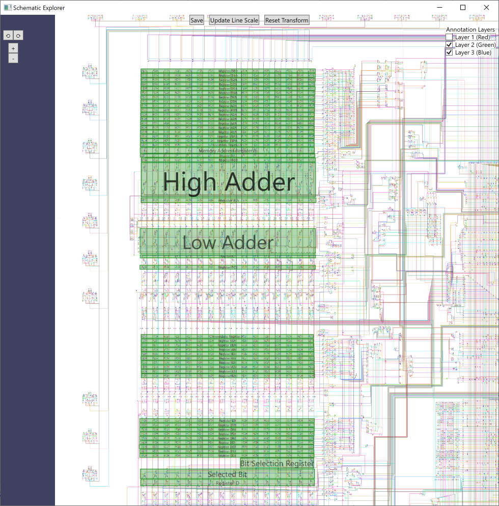
So to confirm, the layers.svg file really contains all the important information, and it was manually created by yourself and quietust by tracing from the die shots. Everything from there, like the schematic and the decoded PLA data, comes from tool analysis from the layer information. That sound about right? One thing I'm not clear on is how exactly do you identify the transistors from the layer information alone. This is probably obvious to some people, but I'm not "getting it" right now. I thought I was figuring it out, but it's not tracking with your schematic, and I haven't come across a good description online about this. I can (and will) tear apart your code soon, but could you elaborate a bit on this aspect? I really want to understand this process top to bottom and document it.
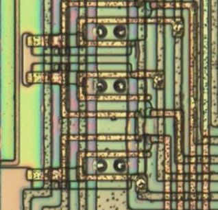
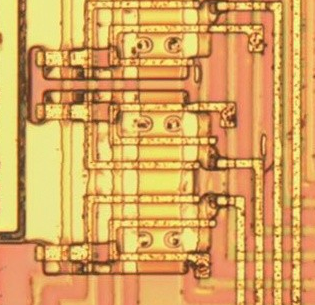
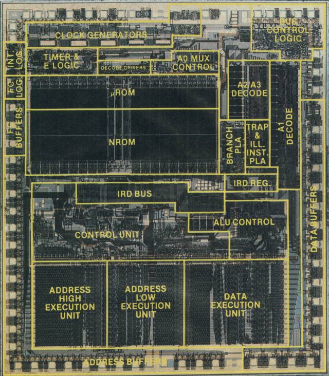
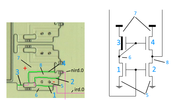
Let me focus on a specific example. Take this region, where the IRD register contents have inverted lines generated and are fed into the A1 decode PLA:
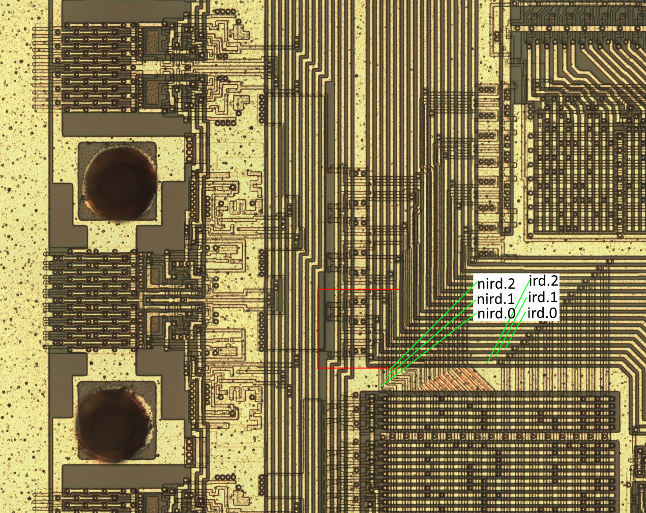
I've annotated the lower three bit lines here, using the same line names you use in your schematic. If I'm following this right, the actual IRD contents are stored to the right of this (but I could be wrong), and this region is simply calculating the logical NOT state of the IRD lines.
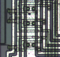
Here's a close-up of the specific region from the original visual6502 decap (containing ird/nird 0-2):
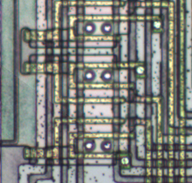
Here's the same region from the newer decap:
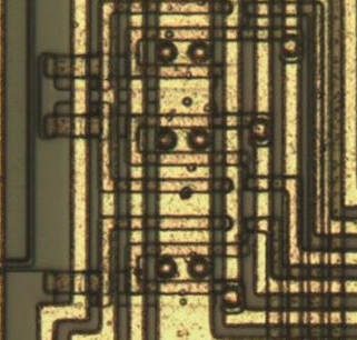
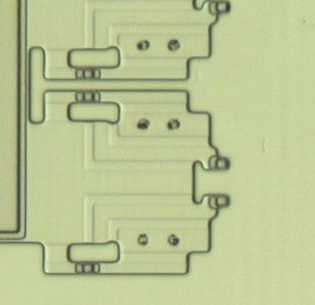
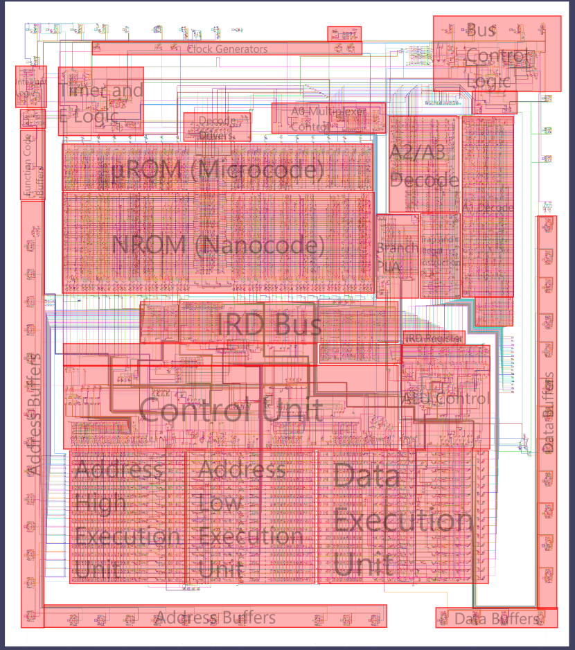
And here's the region again from layers.svg:
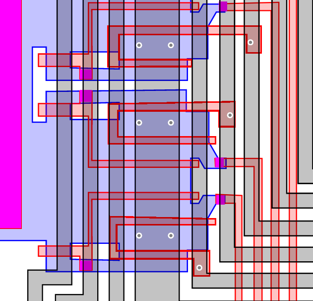
Although I can see how you visually isolate the layers from these images, (which must have truly been a tedious, time-consuming process, so props for doing it!), I don't think I'm properly understanding how you determine the actual transistor logic from what's in front of me. For a single bit line in this region, here's what you show in your schematic:
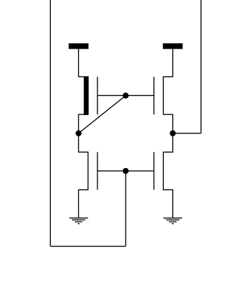
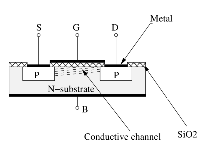
Here we see ird.0 coming in down the left then up from the bottom, and nird.0 going out on the right. Since your clarification about HMOS fabrication (thanks for that) this is making more sense. Based on your description, I assume the MOSFET here with the thick line on top is a depletion fet, which if it's always open acting as a pullup as you described, this logic functions as I'd expect. The ird.0 line is routed to the gate of the two lower enhancement mode MOSFETs, grounding them when ird.0 is true, which forces nird.0 to false. When ird.0 is false, the gates are closed, leaving the pull-up fet to lift the gate of the fet on the top right, which without grounding ties nird.0 to +5v setting it to true. That makes perfect sense. How do you get from a visual inspection of the layers shown above though, to this schematic?
Another question too, in terms of the die shots themselves, where did they come from? I know you said in the past the ones from the visual6502 guys weren't high resolution enough. You've got a series of four higher resolution die shots from decapping through stages of delayering. Did you arrange those ones yourself, or do they come from some other source? Not really important from a technical perspective, I'm just curious.