TascoDLX wrote:A minor gripe:
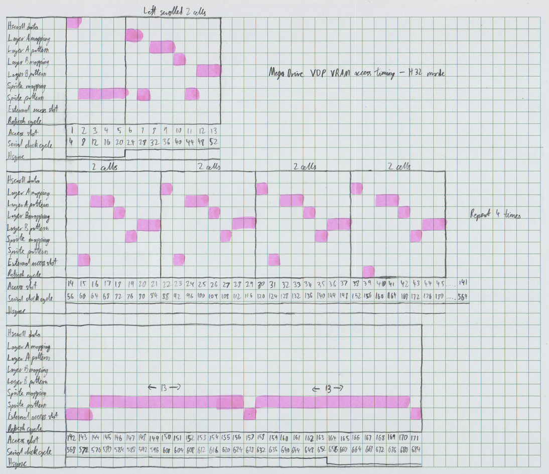
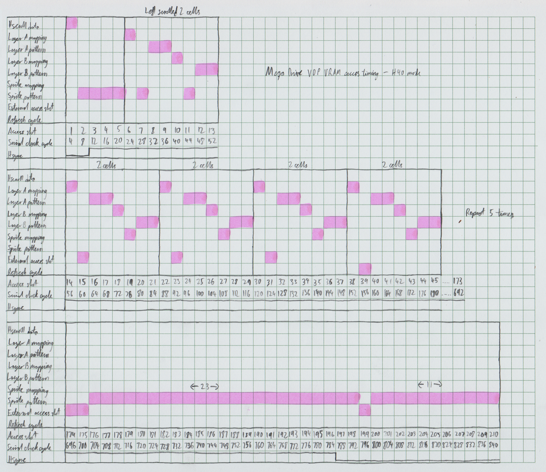
The manual says the maximum wait time for VRAM writes (to a full FIFO) is 4.77us in H40 mode. Let's see: SC in H40 mode is MCLK/4, outside of H-sync. Because of the refresh cycle, there's a gap of 16 access slots between external access slots. So, that's a maximum wait time of 4/MCLK * 4 * 16 = 4.77us. Good.
However, according to the new data, the largest gap is actually 26 slots, and half of that is during H-sync with the overall slower clock. Maybe you have some thoughts on this.
I'd say the manual is simply incorrect. My measurements from the VRAM bus are pretty definitive. My logic analyser is powerful enough to sample all bus activity over an entire hscan line at once, so my reading of the bus activity is accurate. I haven't had to fill in any blanks or take guesses, just observe and record what the actual VDP is doing during operation.
TascoDLX wrote:Also, from the manual, it's pretty obvious that on V-blank lines it's all external access slots except for the usual refresh slots (H32: 167+4=171 ; H40: 205+5=210).
Correct, although I want to look a bit more into the bus activity on the very first and last active lines of the display. I know that the VDP becomes available for user access when it reaches the two back-to-back external access slots on the last line, and it becomes unavailable at that same point on the line before the first line of the display. I have some unanswered questions about sprites though. Does anyone know for sure if you can actually display sprites on the very first line of the display? If you can, the VDP would have to start parsing the sprite list before the first line, or parse it during the last line of the previous frame and carry it over to the next frame instead, otherwise, how would it know the sprite mappings for the first line? Usually the list of sprite mappings are built up in the previous line, but for the first line in the display, there is no previous line.
Another thing I need to confirm is what the VDP does when interlacing is active. One thing I can tell you is that when the "shorter" lines which occur during vsync happen, the refresh slots stay the same, IE, the bus activity is unaffected. During interlacing, the number of shorter lines in vblank is odd however, in order to displace the raster position on the following field, so I want to check what the VDP does in this case, since it would need to adjust the bus timing somehow to "resync" the bus access with the start of a line.
TascoDLX wrote:Now if we count the lines in NTSC, for instance, we have 224 active + 36 blank (that's according to the manual). So, 2 lines remain (or 2.5, in case that means anything). There should be 80 slots in H40 mode used to cache the sprite table, or 64 slots in H32 mode, but what other than that? Perhaps I'm forgetting something. Is there anything else going on there, or is it just bonus time?
The entire sprite table is never cached (that we know of). The VDP latches and stores the first 4 bytes of each sprite mapping in an internal cache as they are written to VRAM, but that cache is never invalidated and re-loaded from VRAM, which is why changing the sprite table address register results in the data from the old location being used. To my knowledge, at this point, I don't believe any VDP access to VRAM occurs outside of the active scan areas, apart from the refresh cycles.
Eke wrote:Some hypothesis:
-> Sprite overflow flag is probably set at the end of this line, if last link is != 0.
-> Sprite collision flag is probably set during HBLANK, when the internal buffer is filled. Maybe it can be set if the internal buffer has not been cleared entirely on previous line (display disabled during active line)
This is something I am going to very specifically test. It ties into this comment:
Eke wrote:I will also try to relate your data with HCOUNTER, which would be better use for emulators than the HSYNC signal.
One very cool thing that's important to note is that the VDP outputs the value of the status register live. What that means is, if the M68000 is in the process of reading the status register, and the value of any of the bits change while the data lines from the VDP are being asserted reporting its current value, the data lines immediately change to reflect the new value. I know from previous testing that the same is true of the hcounter. This means, I can get a cycle-accurate reading of the digital properties of the VDP, such as the status register and hv counter, and determine the exact SC cycle they change, and therefore how they relate to the analog output of the chip as well as VRAM bus access. This is my next project. I've successfully sampled the timing of the hblank flag relative to hsync now, for example. I'll post more information on how all these signals correlate when I've completed this next phase of testing.
Eke wrote:Remaing questions would be about the other RAM access. I think the VDP used a shared bus and wouldn't be able to access them at the same time so CRAM/VSRAM access slots must fit somewhere in that scheme (at least, external acces slots are obviously shared).
CRAM access are most likely done on each pixel, once priority controller output a CRAM entry value but it would be interesting to figure when VSRAM access are done on a line regarding VRAM slots.
This could also helps explaining the weird stuff hapenning to the left-most column when horizontal & 2-cell vertical scrolling is applied at the same time. I don't relly know how this could be accurately measured though
Yep, I'm going to look into this too, but I haven't thought too much yet about how I'll measure it. Oh well, I'll find a way somehow.
Eke wrote:Another thing I'm curious about is the parrallel/serial access thing. VRAM can use both type of access and it seemed to me only the second use the serial clock. I would have thought that that mapping data was addressed using parrallel mode and pixel data using serial mode and that access slots might not been all the same...but I guess you will describe this more precisely later
One of the most surprising things for me when analysing the VDP VRAM access was to discover that, although the VRAM is dual-port, the VDP seems to ONLY use serial access. The VDP never uses the RAM port at all. Since the serial bus provided enough bandwidth, and allowing external access during active scan wasn't a priority, I guess they opted for simple and just used the serial bus for everything. Coordinating parallel access to both ports would have no doubt increased the complexity of the VDP.
HardWareMan wrote:Also, I've been discovered that VRAM signal "SC" (yellow, clock for SIO) is EDCLK (blue).
Correct, when H40 mode is active, SC is equivalent to EDCLK (or, more specifically, when bit 7, RS0, of register 12 is set. Bit 0, RS1, affects the digial operation of the chip, enabling the drawing of a 40 cell display, while RS0 affects the analog operation of the chip, affecting the clock signals and analog video timing). When H32 mode is active, SC is equivalent to MCLK/5.
HardWareMan wrote:And RAS-CAS cycle according to EDCLK:
That's when the VDP is setting up a read. One SC cycle sets the row, the following SC cycle sets the column, then one cycle delay, then the first nybble of the data is moved over the serial bus on the following clock cycle. For a 4 cycle read (reads 4 bytes, because VRAM chips work in parallel, 4 nybbles from each), the read cycles overlap, so when RAS is next asserted, the second nybble of the previous read is only just being moved over the bus, and when CAS is asserted it's the third nybble, and when there's the one cycle delay, the last nybble of the previous read is sent, then the next read is processed, so the serial data bus can read one nybble (1 byte combined) every SC cycle without any gap between successive reads. Writes can't overlap with reads, so a write cycle can only manage to transfer 1 byte in 4 SC cycles.
Note that even when the bus is "idle", it is still transferring data. The VDP just runs off and reads the next successive value from VRAM when it has nothing to do, so in reality, the VRAM bus is always active transferring something, the VDP just doesn't always use the result.
HardWareMan wrote:Also, I saw CAS_before_RAS refresh cycle, but I don't know, where in raster it is (more than 2 ray oscilloscope required).
Those will be the refresh slots I've marked on the timing diagram.