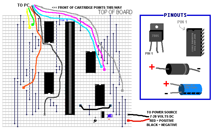
ROM COPIER PLANS V1.00
(c) Cyan Helkaraxe 1999-2000, All Rights Reserved

NO PART OF THIS DOCUMENT (OR ITS FILES), THE DESIGN (AND RESULTING PHYSICAL FORM) OF THE HARDWARE, ANY PART OR THE ENTIRETY OF THE SOFTWARE, OR ANY OTHER RELATED COMPONENT OF THE ROM COPIER PLANS MAY BE COPIED, MODIFIED, CLAIMED AS YOUR OWN, SOLD FOR A PROFIT, OR DISTRIBUTED IN ANY WAY OTHER THAN THE ORIGINAL ZIP FILE.

INTRODUCTION
This document aims to describe how to make a ROM copier device for the Sega Genesis games console using readily available components.
The device in question consists of 4 ICs, a few other components, and a link to the PC's parallel port -- making these plans quite possibly the simplest ever devised.
What's more, the design of the board has been optimized for ease of building, letting the software do the hard work, rather than the constructor, which saves a lot of time and effort when making and testing the device. To my knowledge, no other ROM copier is quite this versatile.
This ROM copier is provided with a software package with MS-DOS, specially written for the purpose of dumping ROMs reliably into .BIN files for use with emulators or any other applications. Some basic testing functions are also provided, so you can be sure that the copier is operating to its fullest potential.


  • The internals of a Sega Genesis cartridge


    COMPONENTS NEEDED
    Here is a list of components required to build the ROM copier.
    All the components needed to build this device should be available from any good electronics store.
    The UK supplier I used was Maplin Electronics, and they can supply goods mail order, as well as having most items in their shops.
    I recommend you get the parts from here if you live in the UK; although they may not be the cheapest or the best, I have built the device from components ordered from here, and it does work. Parts from other stores may differ slightly.
    I've listed the quantity required, followed by the part number, then a description, so for the list item:
    1 x 1N4001 Rectifier Diode
    the 1 x at the start indicates that one is required, the 1N4001 is the part number -- these are mostly an international standard -- go into any electronics store and ask for a 1N4001 and you are sure to get the correct item. The description "Rectifier Diode" refers to what the item is -- be sure to quote the description when ordering too, otherwise there is the danger that the wrong item may be ordered by mistake.
    Remember: the staff at most electronics stores are as intelligent as your average Windows user -- therefore they are only capable of reading text off a screen and comparing it to what you've asked for -- they don't possess any level of knowledge therefore you shouldn't expect them to know what you are talking about, or be sure that they will pick the right item purely with just an order code. CHECK YOUR ORDER TO MAKE SURE IT'S OK, AND IF YOU CAN GO TO THE STORE TO BUY THE ITEMS, DO SO, AND LOOK AT THE ITEMS TO MAKE SURE THEY ARE OK BEFORE LEAVING!!!

    Click on an item to see a picture of it:

    SEMICONDUCTORS
    ==============
    1 x 1N4001 Rectifier Diode
    1 x 7805 +5 Volt Regulator IC
    2 x 4040 CMOS 12-stage counter IC
    2 x 4512B CMOS 8 channel multiplexer / data selector IC


    CONNECTORS
    ==========
    4 x 16 pin IC sockets (standard type -- nothing funny please...=)
    1 x 9v PP3 Battery Holder (type with wires leading out of holder)
    1 x 25-pin D Plug (solder type, male pins)
    1 x 62-pin edge connector, 0.1 inch spacing, double sided -- sometimes referred to as 2x31 way.
    NOTE: If the above item is unobtainable, then get a 66-pin connector (or more) instead, and follow the plans for trimming rather than splitting. If a 64-pin connector is available, then use that -- that one doesn't require any trimming, but it is very rare.

    MISC
    ====
    1 x PP3 9v battery
    <(to fit the holder -- a rechargeable one will do, as will a normal alkaline one -- omit this item if you plan to risk everything and use a power supply!)
    1 x 100MFD (microfarad, sometimes written as a funny u symbol =) capacitor, at least 25 volt rated
    1 x Stripboard
    (39 copper strips, 117 holes in each strip is the one I used, but the smallest you can get away with is 38 copper strips, with 44 holes in each strip, providing the board is completely undamaged at the edges)

    CABLE
    =====
    You'll need 7 lengths of wire going between the parallel port and the board. Make these long enough so that you don't have to throw the copier round the back of the PC when using it -- about 2 meters per length of wire will do, although the shorter the better -- the ROM will have to be read more slowly if the wire length grows, because errors can creep in.
    It helps a LOT to choose 7 different colors of wire, so that you know what goes where on the board.
    You'll also need an extra 2 meters of wire (any color) to use for the wire links on the board itself.
    The choice of wire is up to you -- but make sure it is quite thin. Solid core is easier to solder to the board, but has a tendency to break if handled too much (especially breaking off the board) and is very stiff, whereas stranded core is easy to handle, but a pain to solder. You'll need solid core to do the wire links though -- it's very hard to use stranded core for this purpose.


    TOOLS
    =====
    What tools you use is up to you, and how shoddy you want this to turn out, but there are a few you need:
    A Soldering Iron (ideally low wattage, and small pointed tip)
    A length of rosin core solder (standard stuff -- make sure it is electronic solder, not plumbing solder -- we don't want fat Italian plumbers invading the copier, after all! =)
    Small hacksaw or other cutting device -- a file might be needed, too.
    It helps to have sand/glass paper or some other abrasive material to scrub the board clean before use -- unless it is completely dirt free, then soldering will become a problem, and faults may occur.
    Wire cutters are a must, as are wire strippers (you can use your teeth, but don't blame me if you spend the rest of the year in the dentist's surgery!)
    A Track Cutting Tool, drill bit, sharp knife or something to cut the tracks of the board with. You can buy a dedicated track cutter at an electronics store quite cheaply, and it's worth it.


    CONSTRUCTION
    To construct the device, it is recommended that you follow the pre-made board plans, rather than improvising around this plan -- at least this one works!
    Firstly, before you begin, prepare the work area, and gather all the components together, and verify that you have all the correct ones. For cutting the connector, it is recommended that you prepare a piece of paper on the desk so that all the plastic shavings created can be safely and easily disposed of -- plastic shavings are often sharp and can cause cancer if ingested or inhaled.

    STEP 1
    Clean the board ready for soldering. Use the abrasive material to rub firmly against the copper tracks on the underneath of the board, and only stop when the tracks are completely shiny and free of any dirt. Do not go mad -- you could risk wearing the copper off the board. Be careful around the edges -- it is easy to catch the edge of the board and tear a track up in some cases.
    Even if the board doesn't look dirty to you, clean it anyway -- you'd be surprised how much dirt or oxide there is even on a new board.

    STEP 2
    Now, assuming the beard...uh, board is clean, the next thing to do is to trim the connector to size.
    If the connector was of the 64-pin variety you may skip this section as it is already the right size.
    If the connector is 62-pins (recommended), then you must split it in the center to make two smaller connectors, which should be soldered on the board one track apart. Here's how and where it should be trimmed:

    The fact that the connector is shown on a grid is purely for alignment purposes, and does not imply that you should trim the connector on the board.
    Warning: Be extremely careful when doing this -- it is easy to break the connector by tearing one of the metal pins inside accidentally, or trimming it in the wrong place. Make sure you cut down in between the two metal pins either side of the split, otherwise you will damage a pin, and risk the copier not working.
    The best way to cut the connector is to start by counting along the correct number of pins to find where it needs to be cut. Now, using the hacksaw, make a small notch in between two of the pins, and make sure this notch is fairly deep. Now, do the same for the top of the connector (where the cartridge goes in) to make sure there is a mark each end. Now, cut along the side of the connector to join the notches up. It's best to do this rather than cut from the top downwards. Once you've made the slot deep enough so that you can see through to inside, then repeat for the other side of the connector (making sure that it is perfectly aligned with the other side).
    Now, you may find that the connector breaks apart immediately. If not, then simply break the two halves by hand -- now that it has been weakened it should be easy to do.
    Here is a diagram to show how it is cut:


    Once cut, ensure that the pins exposed at the edges are perfectly aligned -- if they are hanging out at a funny angle then push them back again. Look from the top of the connector into it, to make sure the pins at the edges look like the others, and move them by hand or using a small screwdriver if needed.

    If your connector is 66-pins, then you should cut one end off so that there are only 64 pins (32 on each side) and make sure that the pins present in the place where the split occurred above are completely removed, so that this connector functions in the same way as the above one. When using a connector trimmed like this, take extra care when inserting and removing cartridges -- with one end missing, there is nothing to ensure that it is lined up correctly.
    This method is not recommended, so it's best to follow the above method.

    STEP 3
    The next stage is also a stage involving the connector, and specifies the removal of the unneeded pins. This MUST be done, otherwise you could damage your cartridge and the ROM copier certainly won't work with them present. The pins must be completely removed -- it's no good simply not soldering them in, because they will still make contact every so often.
    There are several ways of trimming the pins, but the most popular involves bending the unneeded pins out at 45 degrees, and cutting them very close to the body of the connector. Another way of doing it is to simply bend the pins back and forth until they break -- make sure they break at the right place though! You could not cut them at all, and instead poke them out at 90 degrees, so they don't go through the holes, but make sure that they don't touch anything else on the board!
    Assuming you have a split 62-pin connector, then these are where the pins should and should not be present.
    Note that if you have a 64-pin connector (including a trimmed 66-pin connector) then you must remove the pins where the split is.
    The image is shown on a grid so that you can see how the pins are aligned -- this does NOT imply that you should trim the pins when mounted on the board!


    It is extremely important that you cut these connectors the right way around! Notice how on the diagram the two connector halves are together. Now, make sure that the two ends facing each other are the ends which have been cut, and the ends which are pointing outwards are the proper, uncut ends. Once you've positioned your connectors like those in the diagram with the two cut ends facing each other, then you may cut the pins. Make sure that you cut the connector's pins by looking at the bottom of them (not from the top down as you will see a mirror image) and make sure they are the right way up (so that the 14 pin section is at the bottom, and the 17 pin section is at the top, just like the diagram). If you cannot hold the connectors in these positions, then either cut one at a time (making sure you know exactly which way round they go), tape them together, or put them on the board and cut the pins. Note that if you are cutting the pins on the board, you won't be able to cut the entire pin off, because of the thickness of the board. Cut what you can and then remove the connectors and remove the rest of the mostly-cut pins.

    Note that some pins, after cutting, especially those close to the edge, might be very weak, and the actual spring connectors might come out quite easily. If it is a severe case, then simply remove the spring connector (making sure that it isn't one that's needed -- i.e. one with a cut pin), but if possible try to push it back into place.


    STEP 4
    At this point, you may fire up your soldering iron and prepare for soldering. The first thing to go into the board will be the connector that you trimmed.
    You need to place the connector in the correct place on the board, so make sure you count along a certain number of holes and place it in. You can see where it needs to go by looking at the board layout:

    You can see where it needs to go -- it is the long, double, vertical strip of pins in the middle, with many missing. The large groups of pins (there are four groups of two lines each) either side of the connector are the ICs, so ignore these for now.
    Make sure you don't get confused and put the connector in the wrong place -- it's easy to mistake one of the ICs for the place where the connector goes on the above diagram.
    As you can see, the first pin (top left, marked with a blue dot, and an A) is on the third track down, and the 20th hole along from the left. A hole is signified by a gray line crossing a black line. The black lines represent the copper tracks, and the gray lines represent the "invisible" lines of holes vertically, used as an alignment aid.
    Note that where the gray lines cross the black lines there is a hole -- even right at the edges, so the very first vertical gray line on the left signifies a column of holes -- as it happens nothing is soldered into this column. Also, there are a number of blank vertical lines to the other side.

    Ensure that you are looking at the board from the BOTTOM (copper side) when counting along, and when you've found the correct hole, place the connector's first pin in it, so that all pins are sticking through pointing at you. Make sure that the connector body is on the TOP side (non-copper side), and the pins stick through to the BOTTOM side.
    In other words, pick up the board so the copper side is facing you. Now, the side you are looking at should resemble the above plan as closely as possible. However, all components must be inserted from the other side so that the pins poke through to the copper side.

    At this point, you have inserted the first component. Because of this, the board is no longer a featureless item -- it matters which way up it goes. Look at the board from the bottom (copper side), and assuming it is the same as in the above plan (all the connector's pins are in the right place) then make a mark in the TOP LEFT corner using a marker pen, or even a knife (make sure you don't get any bits of copper falling across tracks). Now you've made a mark, you now know which way up the board should be for future reference.

    Make sure you put the connector in the right way -- now you've trimmed it, there is only one way round it can go -- check to see if the missing pins line up with the ones on the diagram.
    The 14 pin section of connector should go at the bottom, and the 17 pin section of connector should go at the top. Make sure that the two cut ends are facing each other, and the two "proper" ends are pointing toward the edges of the board.

    Make sure that it really is in the right place -- double check it, and make sure that both rows are inserted -- the first line should be in the 20th hole across, and the second line should be in the 23rd hole across. Again, make sure you are looking at the board the right way round (from the underneath, copper side, with the components going in from the other side) -- if you count from the wrong side, the project will be ruined!

    If your board is more than 38 copper strips with 44 holes in each strip, then it won't be the same size as the one on the diagram, although it will still be usable. If this is the case, simply ignore the extra holes/strips.
    However, the extra area of board that you discard must be known -- it's best if you use the top left most area of board (looking from bottom/copper side) for doing your work, and discard the rest. You may want to mark the discarded areas somehow -- probably by drawing a marker pen or knife line to separate it, or you could stick disk labels over the unused areas to section off a 38 copper strip area with 44 holes in each strip.
    See this diagram for how you should section it off:


    See how you can simply partition off a section in the top-left corner (looking from copper side of board) and discard the rest -- but be sure always to do your hole counting from the top left side. Note how the top corner of the working area coincides with the mark you made.

    Now, if you have any sticky tape, then tape the connector in place so that it won't fall out, and all the pins are sticking right the way through. If you don't, then hold it in place by hand.
    A trick you can use to keep it in place easily is to bend some of the pins outward, so that they can't slip back through the holes.

    It is important that you realize that the two connector halves should be placed one track apart from each other. You can see on the diagram, around the middle, there are what appears to be two missing pins next to each other. This is where the gap is. If you are still unsure, consult the pin cutting diagram again:

    See how the two connector halves must be placed on the board with one copper track gap in between them. You can be sure you've got it right if the pins line up perfectly -- if the first (top left) connector pin is on the 20th hole across, 3rd track down, and the last (bottom right) connector pin is on the 23rd hole across, 34th track down then you've got both halves in the right place. Again, make sure the two cut ends are facing each other, and the track the gap is on is track 20.

    When the iron is ready (test it by seeing if it easily melts solder), wipe it clean using a damp cloth and solder the connector in to the board. Take extreme care to make sure that the solder doesn't run onto another track, thus causing a short-circuit between two isolated tracks. Always keep checking the gaps in between the copper tracks to make sure no conductive material is resting across them.
    Also, make sure that you don't put too much solder on, and it doesn't run too far to the left and right of the connector -- the holes either side of the pins should really be NOT covered with solder.
    The best way of soldering is to apply the iron to the joint between the pin and the track, and then using the other hand, stick a length of solder in the junction, and it should melt and flow around the pin and the track, assuming you are soldering in a horizontal position. You need to hold the iron on the junction for about one second before sticking the solder in, and you generally need to feed about 1.3 centimeters of solder in for each pin. Hold the iron on the join after you've finished delivering the solder for about one more second, and then gently remove the iron, being careful not to spread solder everywhere. Wipe the iron and repeat the process for the other pins, taking care not to touch any other pins with the iron while soldering one of them -- if you do so then the solder may run across the tracks.

    Now, assuming you managed to solder the connector in OK (without missing any pins or making a short across two tracks) now its time to check it against the board layout. Make sure that every pin is soldered, and every pin that needed to be is cut. Ensure that no bridge is made between any two copper tracks, and make sure that the solder hasn't run into the wrong places.

    Make sure that you pay close attention to the angle of the connectors when soldering. Some boards come warped, and often the connectors have some small pegs at either end, so that when you solder it in, the connector halves would not be level. Just before you solder, you can make small changes to the height of the connector at each end so to make the top of the connector completely level. Look at the board from the side and check along the top of the two connector halves -- both should be the same height and it should be a straight line, if not then make adjustments. It's not too critical, but it might cause errors in the copying process if it is badly aligned.

    Ensure that the solder joints are good. Here is an example of various soldering issues:


    With example 1, there is not enough solder on the join, and the wire is poking through the hole, hardly secured by solder.

    With example 2, the join is probably as good as it can be made. There is just enough solder to surround the wire/pin and secure it perfectly to the track, while not being too much so to interfere with other holes.

    With example 3, the join will probably work, but it isn't perfect, and could cause problems later. The wire could well be loose inside the solder without you knowing. If you get a join like this, just re-heat it and see if it cures. You may need to use a solder-sucker or desoldering tool to remove what solder there is and start again. However, if you can't easily fix it, then it'll probably work, but joins like this will be the first suspect if the copier doesn't work.

    With example 4, too much solder has been put on, and it has run across to cover other holes on the same track, meaning it will be hard to put another wire in the next hole (you'd have to heat the blocked hole while pushing the pin/wire into it, so that it melts the solder and lets the pin/wire through). Also, watch out for shallow solder joins -- if there isn't a definite bump with a quite sharp point, then the wire may have slipped out slightly during soldering, meaning that it is probably not being gripped by the solder.

    With example 5, this is probably one of the worse soldering jobs ever -- probably something you'd find in a Microsoft mouse. The solder has actually flowed across on to the nearby tracks and is causing a short circuit. This _will_ cause a problem, and may cause damage to the copier, the PC or the cartridge if you run the copier with it in this state.
    Solder bridges, as they are called, can be hard to remove -- a solder sucker is ideal, although sometimes you can get away with running the iron's tip along the gap in between the tracks (make sure the iron is free of solder when you do this, so wipe it on cloth or sponge first) and through the middle of the bridge. Note also that solder bridges can occur across a cut track, and make sure that this doesn't happen -- if a cut track is bridged, then it won't work and could cause damage.

    With example 6, there is also a large risk. It isn't as obvious as the other ones, but if you look closely you can see something resting between the tracks. Because this is quite light in color, it's a good guess that it is something conductive, and it'll blow everything up by causing a short every bit as bad as example 5. Make sure you CAREFULLY remove something like this -- you may need to pick it off the board with a screwdriver as it may be stuck, but make sure you dispose of it carefully, as it may drop across some other tracks.

    An issue to bring up here is that not all connectors are the same as the one shown in the diagram. The one I've shown has a gap of TWO holes in between the pin lines, although some connectors may only have ONE hole gap.
    This isn't much of a problem -- it'll make the tracks slightly harder to cut, but other than that it's OK. Do watch out for counting the other components wrongly though -- now that there is one less column of holes vertically, it would be easy to get things in the wrong place. It's best to insert a blank vertical column of holes just to the right (when looking at the bottom of the board) of the connector, to compensate for the missing line in the middle. This means that the connector will still occupy 4 columns, but one of these is a blank line. In other words, place the connector in the same place as the picture of the board. The pins to the right (looking from bottom) will obviously be one hole too far to the left in this case, although the left hand row of pins will be in the correct place. Just insert a blank line to the right of it.
    To clarify this, here's a modified board plan (refer to this instead of the other plan if your connector is the smaller sort):


    STEP 5
    The next step is to cut some of the tracks. On the lower board plan you can see where the track breaks need to be:


    The track breaks are signified by a short break in the horizontal black lines (representing copper strips). You can see them in between ICs and between certain pins on the edge connector.
    Now, here I've placed the breaks directly in between two holes. While this is fine if you are using a knife to cut the track (you can simply cut out a section between holes this way) it isn't so easy to use a track cutter to do this.
    If using a track cutter, place it to the immediate left or right of the place where the track is to be broken. You can see that for every track break on the diagram there is at least one hole to either side of the track break -- place it in either of these places. Make sure it is on the same track though -- while you can move left and right, you cannot move up and down.
    Now, to cut the track, simply twist the track cutting tool (or drill bit, depending on what you are using). The track cutter's drill-like bit is far too big to go through the hole, so when it is turned it scrapes away the copper track from that small area -- and it does its job by isolating the two sections of the track. Make sure that all the copper fragments are carefully brushed away and discarded -- they conduct electricity so if they stick to the board then they might short something out, and if they drop into some other electrical equipment the results would be memorable.
    If you don't have a track cutter, then a drill bit is the next best thing. One that's roughly 1/4 of a centimeter in diameter will do -- just use it in the same way as the track cutter, although it is harder to use. Fitting the bit into a hand drill may help. An electric drill will devastate the board.
    If using a knife, make sure it is very sharp and place two cuts in the track next to each other, and peel a small segment of the copper away -- that will do the same thing, but it is harder to get it right. A small flat-bladed screwdriver may be the best bet for economy track-cutting; all you need do is use it in the same way as the track cutter, and hope that it scrapes the track away enough. Here is what a cut track should look like:

    If you can't get it that good (perhaps there's not enough space between the two soldered joints) then something like this will probably do:

    However, as usual, check the result extremely carefully to make sure that there is no copper resting across the break, and to make sure that the copper hasn't twisted and shorted against adjacent tracks.
    As usual, be very careful to dispose of the bits of copper carefully, rather than letting them get stuck to the board.

    To start with, at this stage, only break the tracks in between the two rows of connector pins -- as you can see there are 16 tracks right in between the two rows that need breaking -- this is to stop certain pins next to each other being connected to each other.
    Once these tracks are broken, you may move on to the next stage.
    If you have a suitable measuring device, then it is best to check to see if all the tracks are indeed broken, or failing that, look at the breaks very closely (with some magnification ideally) to see if there is any problem.

    If you find track cutting difficult because solder has flown across the parts that need cutting, then simply cut the tracks before soldering. However, it is recommended that you cut the tracks with the edge connector mounted in the board (even if it isn't soldered) so that you know where it needs to be cut exactly.


    STEP 6
    At this point, you should have a successfully soldered edge connector with certain tracks in between broken. As always, check your work to make sure it is perfect and everything is as it should be on the board plan.
    The next thing to do is to solder the ICs and IC sockets in. The first IC to be soldered should be the voltage regulator IC. This IC looks like a power transistor -- it is a small (1CM2 or so) plastic square with a metal tab with a hole in it poking out the top. This IC has 3 pins, input, ground, and output.
    The part number for this IC is 7805. The 78 signifies that it is from the standard 1 amp range of positive voltage regulators, and the 05 signifies the voltage it outputs. Make sure that your IC has this number printed somewhere on it -- it may be surrounded by letters and other numbers, but make sure it is a 7805.
    Like the connector, it is critical that you put the IC in the correct way around. This isn't because you have to cut certain pins (and indeed you should NOT do so -- all the pins are needed) but it's because each pin on the IC performs its own unique function, and it has to be in the right way.
    Unlike the other ICs, no socket is readily available for this IC. Therefore you will have to take extreme care when soldering it in -- the reason for the sockets is so that you can't risk overheating it. ICs are very prone to being overheated, and they can be ruined this way -- if you solder the sockets first and put the ICs in when you are finished, there is no danger.
    Because the voltage regulator IC doesn't have a socket, make sure that you take no more than 6 seconds soldering each pin of the IC. Also, after soldering one pin, give the IC a 15 second break to cool off before you move on to the next pin. There are only 3 pins so this won't take long.

    All the ICs on the board have a yellow dot in one corner (on one of the corner pins). This yellow dot tells you that pin is pin 1. ICs all have numbered pins, and obviously, pin 1 is the first one. If you know you've got pin 1 lined up, then you can be sure that the IC is the right way around.
    So, how do you know which is pin 1 on the IC itself? Have a look at the following diagram and you'll see. The diagram shows two things -- what the board should look like when completed, and the pinouts of the ICs.


    You can see the 7805 voltage regulator IC in the PINOUTS box. This is viewed from the front of the IC, with the plastic cube pointing towards you and the metal back pointing away. When looked at like this, you can see that pin 1 is on the left.
    When you insert the IC into the board, make sure this PIN 1 is aligned with the yellow dot. Make sure you don't get confused by moving the IC around a lot -- as you have to move it quite a lot to get it into the board, it might be best if you get a marker pen or something, and mark that pin when looking at it from the front. Then, you'll know which is pin 1. Make sure you wipe most of the ink away before soldering it though!

    Pick up the board again, and look at it from the copper side (bottom) as before. Also as before, insert the IC from the OTHER side.
    Turn the board so that it is the correct way around -- so that the mark you made is on the top left (as before). Now that you've started building the board, it is important to make sure it is the right way up. Double-check the layout of the pins against the pins in the diagram to make sure it really is the right way up, and move the mark if needed.
    Make sure that pin 1 goes through the hole that's on the 35th track down, and the 11th hole across from the left (looking from BOTTOM of board -- copper side).
    The other pins should be above pin 1, although on the same hole across, they should all be on different copper strips (tracks). Pin 2 should be on track 34, and Pin 3 should be on track 33.
    Make sure it's in the right place -- you can see it on the board plan -- it's the group of 3 pins between the red and green lines.
    Once it's in the right place, solder it in carefully, and you are ready to progress to the next step.


    STEP 7
    Now, it's time to insert the sockets for the other ICs.
    Because they are simply plastic sockets, it doesn't matter which way round they go -- as long as they go in the right side of the board (from the non-copper side, so that the pins poke through to the copper side).
    However, when you put the ICs in the sockets (a much later stage of the plans -- you'll be told to do so when it's time) you have to make sure you get the ICs the right way around.
    You can see where they need to go on the board plan -- they are the groups of 8 pins next to each other (16 pins in total).
    As usual, pin 1 is signified with a yellow dot -- this isn't important yet because obviously you only need to know where pin 1 is when you actually plug the ICs into the sockets.
    However, do make sure that you actually put the sockets in exactly the right place -- although it doesn't matter which way around they go, it _does_ matter where they go on the board!
    Looking at the underside board plan again, start with the top left IC.
    This IC socket has pin 1 in the 13th track down, and the 16th hole across from the left. Make sure all the other pins are below this -- make sure it matches the board plan exactly, so the IC socket occupies tracks 13-20.
    The first line of pins should be in the 13th hole across, and the second line should be in the 16th hole across.
    Again, make sure that you are looking at the plan and the board from the bottom.
    Solder the socket in once it's in the right place and is pushed all the way into the board (because the pins are so short on IC sockets, you have to make sure that it is pushed in all the way to make sure the solder joint will be OK).
    To avoid you having to skip back to the bottom board plan, here it is again:


    Now on to the next socket. The next one is the bottom left IC (from the board plan -- the bottom of the board). Pin 1 of this IC socket goes in track 24, and 13 holes across from the left. The IC should occupy tracks 24-31, the first line of pins should be on the 10th hole across from the left, and the second line of pins should be on the 13th hole across from the left.
    Check to make sure it matches the plans, and then solder the socket in.

    The next IC is the top right one. Notice how the ones on the right are put in upside-down.
    This socket should have pin 1 in track 10, and the 27th hole across from the left. Because it is upside down, the other pins should be above this, so that the IC occupies tracks 3-10, with the first line of pins on the 27th hole across, and the second line of pins on the 30th hole across.

    The last IC, the bottom right one, is also upside-down.
    Pin 1 should be in track 27, and the 27th hole across from the left.
    The IC should occupy tracks 20-27, the first line of pins being on the 27th hole across, and the second line of pins being on the 30th hole across.
    Do not be confused by the fact that this IC's pin 1 is in hole 27,27 -- it really is 27 down, 27 across -- that isn't a printing error.

    Finally, check your work, and make sure the solder joints are good. Now you can move on to the next step.


    STEP 8
    At this point, you should have all four IC sockets, the two halves of edge connector, and the voltage regulator IC soldered into the board.
    Some of the tracks are cut on the edge connector, but there are still some tracks remaining to be cut (not on the edge connector, rather on the ICs).
    At this point, it's best to cut the IC tracks -- all tracks in between the two lines of pins on each of the four IC sockets must be cut.
    You can see how it goes on the diagram -- for each IC there are 8 tracks that must be cut.
    Note that the voltage regulator IC doesn't need any tracks cut at all, although the four sockets do need the tracks cut.
    As usual, follow all the precautions of track cutting as before. You may find it hard to cut after you've soldered the sockets in place, although it is probably harder still to cut the tracks before you've soldered the sockets in place -- if you've got the sockets in place, at least you can tell exactly where each break needs to go. Just make sure that during soldering you don't let the solder run across the tracks too far. You may need to use a knife instead of a track cutting tool if it becomes too much trouble to break the tracks normally.
    At this point, all the in-line components have been soldered, and their tracks cut.


    STEP 9
    At this point, it'd be good to solder in the last components.
    Apart from wire, and the PC parallel port connector, plus any other misc. stuff, you should have two electronic components remaining.
    There should be a diode, and a capacitor. Both of these go near the voltage regulator IC, and that's what they are used by.
    Firstly, the diode. Because the diode is a semiconductor, like ICs, it is sensitive to heat -- follow the same precautions as when soldering the voltage regulator IC to avoid damaging it.
    The diode is the small, black, tube-like device with two wires out either end. To get both of the diode's leads to go though the board in nearby holes, you'll have to bend the leads. Be careful when doing this -- don't try to bend the leads too close to the body of the diode as you'll break them off.
    However you bend it doesn't matter, just so long as the two leads both go through the right holes without ever touching each other, or touching anything else on the board (like wires, or components). Make sure the diode is pushed as far down as you can get it without forcing it -- diodes usually have very long leads, and you won't need all that length, so it's best to push them all the way though the board, and cut the spare lead from the other (copper) side of the board. This way it ensures that you won't have the diode standing high off the board on long leads.
    Here is a diagram of the best way to bend the diode's leads to make them fit through the holes -- don't forget that the holes it has to go though are right next to each other.


    The diode is signified on the board plan by a green line with a dot at each end.


    You can see it right at the bottom next to the voltage regulator IC.
    Each dot shows a "pin" of the diode. Basically the line shows that the diode connects between those two points.
    Note that you must insert the diode the correct way around -- it's easy enough to tell. If you examine the diode, there is a positive side and a negative side. How do you tell? Well, basically there is a small white ring around one end of the diode -- the lead this ring is nearest is the negative side. Have a look at the pinouts of a diode:


    Hopefully now you should be able to determine which lead is negative, and which lead is positive simply by looking at the diode. Now, you need to know which way to insert it in the board.
    The green line, if you look closely, is actually made up of two halves -- a bright half, and a dark half. The bright half signifies the positive side, and the dark half signifies the negative side.
    In addition to this, there is a small + symbol marked next to the hole where the positive lead should go.
    The negative lead of the diode (the lead nearest the ring on the diode body) should go into track 35, and the 13th hole across from the left (looking from bottom, copper side of board).
    The positive lead of the diode (the other lead) should go into track 36, and the 13th hole across from the left.
    Once you've soldered it in (take care to avoid overheating, and make sure it solders OK -- diodes can be harder than some other components to solder) then you can cut off the extra lead. You could cut the extra lead off before soldering, but you may find that it is easier to leave the extra on while soldering to help secure the diode.
    Make sure that the diode is in the correct way around, and also make sure that the leads on the diode don't touch the voltage regulator -- the two are very close, and it could cause a failure if the lead of the diode came in contact with the metal back of the voltage regulator. Carefully and slightly bend both components a bit away from each other, and if needs be, insert a piece of paper or card in between the two, and fix it somehow. Be warned: the voltage regulator can sometimes get quite hot when the copier is in use, so make sure the paper isn't very flammable -- in other words, make sure it isn't coated with some flammable chemical.


    STEP 10
    The last actual electronic component to be soldered to the board is the capacitor. Like the diode, this component goes near to the voltage regulator, although it is on the other side.
    On the "bottom of board" plan, you can see the capacitor is signified by a red line, much like the diode, with two dots, and a light half (also marked with a + symbol) and a dark half.
    With most of the components on the ROM copier, if you put them in the wrong way, it either doesn't matter, or you will risk damaging the copier, cartridge and/or the PC. However, the capacitor is a much more serious issue.
    If you put the capacitor in the wrong way and power the unit up, you could risk the capacitor exploding. Because the capacitor is a sealed container, and it consists of a chemical which if overheated will cause excessive gas to be produced, the pressure will build to an extend where the capacitor will literally explode under the strain. Because connecting the capacitor the wrong way or over-voltaging it will overload it, both are extremely dangerous. If you want the capacitor to explode, then do so at a safe distance, using a dedicated capacitor explosion device -- you will damage the rest of the copier and all connected items if the capacitor explodes on the copier.
    Do not underestimate the force at which a small capacitor can explode with.
    A small capacitor like this one is capable of bursting through card, and at a shorter range causing burns and other nasty injuries. If you are looking at the device wondering why there is smoke coming off of it, then when it explodes it'll go right through your eyeball and fry it, and in fact it may go back even further into the brain and kill you. If you hear the other warning sign that it's about to explode (sometimes it gives you no warning) -- a hissing sound -- and put your ear up to it, then when it explodes, the capacitor will blast into your ear, through your eardrum, and it will smash all the bones inside up, so that you won't be able to hear anything again.
    In fact, you could also die from this.

    Anyway, basically, MAKE SURE YOU PUT IT IN THE RIGHT WAY!!!
    The capacitor itself is marked -- take a look at the pinouts diagram a few pages back and you'll see. The capacitor has two leads, just like the diode. However, most capacitors nowadays have both leads coming out the bottom of the device. Also like the diode, one lead is positive, and the other is negative.
    Another thing in common with the diode (at this point, you're beginning to wonder whether it's a diode in disguise -- but it's not -- the diode is a delicate semiconductor, and the capacitor is a serial killer!) is that the negative lead is marked.
    If you look at the body of the capacitor, sometimes there is a + next to the positive lead, and/or a - next to the negative lead.
    However, most small capacitors aren't this obvious. Nearly all capacitors mark the negative lead with a kind of black arrow pointing toward it.
    The lead which the arrow points to is negative, and the lead it doesn't point to is positive.
    Sometimes this arrow is a row of arrows, or sometimes a black stripe. Sometimes it even features lots of - symbols.
    However, if the arrow is red, then take a closer look -- a red arrow could indicate the positive lead, rather than the negative lead. However, in 18 years I've never seen a capacitor with a red arrow, so you should be OK.

    As before, the positive lead position is marked on the board. Simply insert the capacitor in the correct holes and solder it.
    The capacitor is quite sensitive to heat -- not quite so much as the diode, but if you do manage to overheat it, then it'll explode. Just be careful, as always.
    The capacitor's leads are often longer than they need to be, so make sure you either cut them before soldering (only recommended if you know what you are doing) or after soldering (makes it harder to solder, but it's less easy to make mistakes and muck up the solder join by the capacitor falling out during soldering). You can cut the leads right close to the solder join -- there's no need to keep any lead poking out of the solder join, although don't go cut the solder join itself off!
    The capacitor's negative lead should go in the 34th track down, 9th hole across from the left, and the positive lead should go in the 35th track down, 9th hole across from the left.
    Make sure you are looking at the board from the copper (bottom) side, and you are inserting the components from the other side.
    Double check everything to make sure it is in the right place, and the right way around, and you are ready to move on to the next step, having inserted all the components.


    STEP 11
    Unfortunately, this is the most tedious step of all.
    Basically, you've got to insert all the wire links.
    The idea of wire links is to electrically connect one track to another -- tracks which could be quite a distance apart from each other -- without interfering with the tracks in-between.
    Most wire links are of the jumper variety, although there is one direct wire link. This step will concentrate on getting the jumpers soldered in.
    Jumpers are basically exposed wire (usually solid core) running from one hole to another. The reason you shouldn't use stranded core is because it won't be easy to solder, and it won't be easy to manage once you've stripped the insulation off. Why strip the insulation off? Well, wire links are often very short when compared to conventional wires, and insulation just gets in the way, makes soldering difficult, and makes in bulkier than needs be.
    You could keep the insulation on if you want, although I find it is easier to remove it.
    To make a wire link, it's best to take a length of solid core strip, and strip back a 15CM section of insulation. You may find that's hard to do -- so strip it back in 2CM steps.
    Once you've got 15CM of bare wire, then you can insert one end in the place where the link starts. Then, after pulling enough wire through to the copper side so there's something to solder to (1CM will do), run the wire tight against the surface of the board along to the destination hole. Slightly beyond this point, cut the wire, and poke the end in the destination hole.
    Because you stopped slightly beyond the destination, you've got some spare wire on both the source and destination holes. From the copper side, pull the spare wire through as much as you can to make the wire as tight as possible, and then bend the spare wire over to one side slightly, to stop it falling out.
    At this point, you can solder it just like any other component -- do not touch the wire while soldering it though because heat will conduct along it much quicker than it conducts through components!
    Because the wire is exposed, make sure it doesn't come into contact with any components, pins, or any other wire links.
    Whenever you run out of exposed wire, simply strip back some more (it's best to allocate a section of wire for the links by cutting it away -- otherwise you may find that you go using up all of the wire that is supposed to be used for other tasks).
    Here is what a soldered jumper should look like from the top (non-copper side) of the board:

    (color may vary)
    Here is a whole load of jumpers soldered -- note how they mustn't touch each other:

    (images shown rotated by 90 degrees for ease of display)

    Now, have a look at the board plan again:


    You can see where the wire links go -- they are signified by blue lines, with a dot at each end. Do not confuse them with the blue squares, which are something different.
    The blue line represents the wire link itself -- of course, in reality the wire link would be on the other side of the board, not the copper side -- this is just for illustration purposes. The dots show where the link goes through to the copper side and is soldered.
    Make sure you insert every wire link in the correct place, and double check your work. It's easy enough to do now you've got some other components on the board -- you've got "landmarks", as it were.
    There should be 37 wire jumpers in total.
    Make sure the solder doesn't flow across tracks when you are soldering -- it's easy to do if you bend the wire too far to one side.


    STEP 12
    Now, it's time to do the semi-final touches to the board construction.
    One link remains to be soldered. This is not a normal link, like jumpers are.
    Because there wasn't enough physical room on the board (and to make construction easier) it isn't possible to use a jumper.
    Therefore, two tracks are connected directly by a piece of wire. This piece of wire is just solid core wire, just like the stuff you use for links.
    In fact, this link is very similar to a normal link, except it isn't tight to the board, it's insulated, and it runs horizontally instead of vertically.
    The wire link should be about 8CM in length -- that's more than the distance it has to span, but it mustn't be tight against the board -- it must be able to work its way around the other components.
    Simply take a length of solid core wire, and strip back about 1CM of insulation.
    Insert this bare end into the first hole where the link starts.
    Now, run this wire around (leaving enough slack) to the next hole, and cut it just slightly beyond the destination hole. Then, strip back 1CM of insulation from the freshly cut end, and insert that into the destination hole. Ensure that the bare metal is pushed fully into the board on BOTH ends of the link, and solder it in as normal. After that, cut any spare wire off the solder joint.

    If you look at the board plan, you can see two blue squares, with light-blue crosses in the middle.
    This shows the source and destination holes for the link.
    Both holes are on the 31st track down, the first one being on the 8th hole across from the left, and the other being on the 18th hole across from the left.
    However you choose to run the wire link, make sure it doesn't have to pass over the IC socket which it is close to -- if you do that, then you won't be able to get the IC in!
    Here is a diagram of the finished board (the same pic as before, although this time ignore the pinouts in favor of examining the board):


    Your board should look something like this now, except it will be missing the wires that go to the battery and the PC.
    Before that though, it's time to finish off the track cutting.
    There are two tracks remaining to be cut -- they are (when looking from the bottom, copper side of board) to the left of the connector and to the right of the ICs. one is between the direct wire link you just soldered, and a jumper (near the voltage regulator), and the other is right next to pin 1 of the top left IC. Cut these following the standard precautions, and then you are ready for the final step of board construction.


    STEP 13
    Now, it's time to solder the wires to the board.
    There are two wires for power, and 7 wires to the PC -- it's possible to build the device with only 5 wires to the PC, but it makes the board a bit more complex to build, and it's easier to solder the extra 2 wires than fiddle around with a complex board.
    Firstly, solder the power wires. If you have followed the instructions and are using a battery and holder, then solder the two holder wires to the appropriate holes. You can see where they are on the bottom board plan:


    You can see to the far bottom left two squares -- one is black with a - symbol in it, and the other is red with a + symbol in it.
    For those of you too stupid to work out what next, solder the red battery holder wire (or if it isn't red, the one representing positive) to the red square, and the black wire to the black square.
    If you have broken the rules and are using a power supply or similar, then you can use your own connectors. However, Cyan will impose a $25 fine for everyone who breaks the rules in such an inconsiderate manner.

    Now, on to the PC connectors.
    There are 7 different wires to the PC, and you should have 7 different colors of wire. If for some reason you haven't got 7 different colors of wire (well, there's no excuse really, is there!?...!) then you'll probably have to label them with the color names.
    I've used GREEN, YELLOW, ORANGE, BLACK, GRAY, PINK, LIGHT BLUE.
    If you are using less than 7 colors, then make up paper labels to stick to both ends of each wire, so that you can give them these color names.
    If you have 7 different colors, other than those I've chosen, then either label them as before, or make a conversion chart, so say, whenever I talk about the pink wire, you know to refer to the blue wire.

    At this point, decide on a length for the cable from the copier to the PC, and cut 7 (possibly differently colored) lengths of cable all of the same length.
    If using labels, make them at this point, and make sure you put them on the right wires -- if you make two GRAY labels, then don't go putting a GRAY label on one end of the wire and a YELLOW label on the other!
    Fit the labels about 8CM from the end of the wire -- this means that it won't get in the way, and will be easy to see.

    The next stage is to strip the ends of each of the 7 cables -- both ends of each cable need to be stripped -- expose about 1CM on each cable -- which is 14 ends in total to strip.

    Now, all the ends which go onto the board can now be soldered. You can see where each colored wire needs to go by looking at the diagram -- you can see colored squares. If it's a large square then it signifies a wire of some kind. If the square is blue then it represents a direct wire link (not a jumper, which is signified by smaller squares connected with a line).
    There are 7 (excluding the black and red power squares in the far corner) squares in total for connection of each colored wire.
    As usual, solder carefully, making sure that you push the entirety of the wire down into the board before soldering. If you don't then it'll slip out, and either make the solder join fail, or leave a too large amount of bare wire exposed on the non-copper side of the board, and risk touching other components, etc.
    Cut back the extra wire when you've finished for each of the 7 wires.

    Now, at this point, the board has been completely soldered!


    STEP 14
    Before you turn off the soldering iron, there is one other thing you have to do. Send me $1400 right away -- get in touch with the address. Alternatively you could send me a Roland JV-2080 complete with Orchestra, Orchestra II, and Session expander boards.
    Apart from that, you have to solder the other ends of the PC wires to the parallel port plug (D-plug).
    To do this, you'll probably need to cut the stripped ends down to about 1/3rd of a centimeter of exposed wire.
    Simply place the appropriate wire in the appropriate pin (there's a little "bucket" to hold the wire in place if you're careful) and apply solder and the iron. This should work, but it's fiddly and you have to be quite careful.
    I've designed the system so that the wires are as far apart from each other as possible -- this is to avoid accidentally de-soldering another wire when soldering one (this happens a lot with closely packed wires).
    Solder all 7 wires to the correct places, and then wind the entire assembly in some kind of adhesive tape. It's not the most professional solution, but that's how my entire PC is built, and it's still going.
    You just have to be very careful when inserting and removing the plug -- you have to insert and remove it by pulling on the flanges out the side of the connector itself, not under any circumstances should you pull on the wire or the tape. You may need a screwdriver to lever the plug out when you've finished with it.
    If you want a more professional solution, then you can sort it out yourself!
    You can buy "hoods" for these connectors, so that you can turn it into a proper plug. You could also plug the end (semi-permanently) into a printer extension lead and then plug that into the PC, which has the added advantage that you can keep the leads from the ROM copier to the home-made plug much shorter, and the copy times will be faster.

    Looking from the back of the D connector (the end with the buckets, not the end where it goes into the PC) with the widest part at the top (you can see which way up it is) simply follow this diagram for connecting the wires to the pins on the plug:


    You can see a picture of the prototype's plug here (remember, the soldering is poor, the colors are different, and the angle is such that you can't see properly which wires go where):

    The front view (shown on right) is taken from such an angle that it is hard to see if the connector is male or female. However, it is definitely a male connector -- it has 25 pins, rather than holes.


    STEP 15
    Finally, it's time to put the ICs in. Often, professionals test the board before putting the ICs in using scopes and meters, although if you don't have access to this equipment and/or don't possess the knowledge to do such tests, then simply put the ICs in now -- you'll soon know if it goes wrong! =P
    You can see which way round they need to go by looking at the TOP of the board, and comparing it to the plans of the TOP of the board (that's the picture with the pinouts). You can see on the plans that pin 1 is marked with a yellow dot. Simply align pin 1 on the real IC with the yellow dot. How do you know which is pin 1 on the real IC though? Look at the following pinout diagram:


    You can see that the IC (looking from front of IC, with pins going away from you) has a semi-circular notch at the top, and/or a small dot next to pin 1.
    If the IC features a dot, then it's easy to figure which is pin 1. If not, then it's still quite easy -- when looking at it from the front so that the pins are going away from you, with the notch at the top, pin 1 is the top left pin.

    How do you know which ICs go where then? Well, the two 4040 ICs go at the top of the board diagram (looking at either side).


    Looking from the board this way, the two IC sockets at the top either side of the edge connector (the one at the very top, to the left of the edge connector, and the one further down, with pink and light blue wires nearby) are the ones that have the 4040 ICs.
    The other two sockets -- the one next to the voltage regulator in the bottom right of the board, and the one to the left of the edge connector, near orange and black wires -- take the 4512B ICs.

    It's easy to see which IC is what -- they are usually labeled on the top surface. Look closely at the numbers and letters there -- you should see either 4512B or 4040 depending on which IC it is. Of course, there are other numbers and letters, so you may see something like:
    HCF4512B
    018497AZ93-SGS-T
    As you can see, there is the string of text "4512B" there -- so this is a 4512 IC.

    When inserting ICs, make sure that they go the right way round in the socket (there's only two possible ways, and one is wrong -- check pin 1 on the IC against pin 1 on the TOP board plans), and make sure that you slightly bend the legs of the IC inward so that they go into the socket easily -- don't use excessive force -- a firm press with your thumb should be OK.
    ICs are static sensitive, although these aren't particularly vulnerable.
    Avoid working in static-rich environments -- it's best to touch some large metal area before handling the ICs.
    However, the biggest threat to the ICs is damage via pin bending (if you bend a pin one way, and then another, it will be severely weakened, and will almost certainly break), and mistakes in the circuit.

    At this point, your board should resemble, almost exactly, the device shown in the above, TOP board plans. Make sure you've got the ICs in the right way with a quick visual comparison of the board and the plans.
    Your board (from the top) should look something like this (picture rotated by 90 degrees for ease of display):

    Note that this board (a shot taken from the prototype model) doesn't feature a voltage regulator or a diode, and has an extra wire link next to the capacitor, and is missing some other links. Also, the wire colors are different. However, apart from those differences, they should be almost identical, although in the above picture, some components may be located in slightly different positions.
    I've routed a couple of cables through the break in the edge connector (only do this if your cables are small, and you are sure it won't damage the connector) and all the cables are routed through under the wire links. This serves to hold them steady, without putting stress on the soldered joints, even when I have to move the board. If you do this, make sure that you don't let the heat of the links (when soldering them) melt the insulation on the wire, and make sure the wire doesn't pull the links so that they touch each other.

    Also, you may want to look at the bottom of my prototype board (picture is upside-down in relation to plans):

    The first thing that strikes you is that my soldering is terrible! (hardly surprising -- I'm a musician and electronic *designer*, not builder!) However, extensive visual checks were made to ensure that there were indeed no short circuits occurring. You might see a few solder bridges in this picture -- those are intentional -- in the prototype model (and because I was in a rush) some of the links are replaced by solder bridges.


    STEP 16
    And concluding on a round number (16 -- $10 -- %10000) it's time to do the final actual step in constructing this board.
    At this stage, you could indeed use it, but most people will want to take some kind of precaution to protect their PC, cartridge and board from damage.
    You could install it in a box quite safely -- plastic, or cardboard is fine, although if using metal, you must insulate the board first -- more about that later.
    However, if you put it in a box, it makes things more fiddly, especially cartridge insertion/removal, and battery connecting/disconnecting -- although for the latter you could fit a switch.
    However, the simplest method of effectively protecting the circuit against limited physical abuse, and shorting is insulating it.

    Insulating the board can be done in a number of ways, although I prefer the simple and shoddy, yet highly efficient and economical system. Simply take a sheet of clean paper and place it under the board (so that the copper side is facing the paper). Now, wrap the board up in the paper, and when you are finished, simply use adhesive tape to stick it in place. If you need to, use many sheets of paper. Make sure that you make a hole in the top just big enough to let the whole edge connector poke through, although not being so big that there is a large gap around the edge, with exposed circuitry.
    As for the battery holder wire, and the PC wire, simply route those out the edge of the paper wrap before you begin wrapping.
    Don't operate the ROM copier on a metal surface, or with metal anywhere around it if you can avoid it, even with it wrapped in paper.

    You may wish to use tape to hold the cables in place -- tape them to the underside of the board or something, just so that you don't risk breaking them off the board while handling it.

    Be careful not to bend any of the components over on the board while doing this -- some components are close together, and you'll risk not just the component breaking off the board, but quite possibly it touching another component/wire, and causing a serious incident.

    At this point, you may use your ROM copier.

    Here's a picture of the completed board, shot from an artistic angle(!):


    And a close up of the board with the ROM inserted: (half of the board is obscured due to a strange angle):


    OPERATION
    Now, as you've built this ROM copier, it might be a good idea to use it.
    However, if you built this ROM copier purely so that you could burn yourself on the soldering iron, then you may skip this section.

    The ROM copier is really quite easy to use. At this point, you should have a completed board, with all ICs fitted, and with the PC connector fitted.
    However at this stage the battery should NOT be fitted into the connector.

    The first stage in setting up the ROM copier is to connect it to the PC. This can be done safely with the power on to the PC, because the D connectors used on parallel port connectors are nearly impossible to short out when inserting and removing plugs. Some connectors, like PCI and ISA slots, if you remove the cards with the power on, you have to remove the card fairly square and reasonably carefully, to avoid the card slipping across the slot and risking damage.

    When you are using your ROM copier, you must disconnect any peripheral you have connected to your parallel port at the moment -- this includes scanners, ZIP drives, sound devices, printers, etc. Even if your device features a thru port (so that you can plug another parallel device into it) then you must still disconnect it -- the ROM copier probably won't function properly when plugged into a scanner or ZIP drive thru port.
    However, good parallel switch boxes (mainly only the manual ones -- not automatic digital ones) may be of use -- this way you can select between the copier and your other devices without having to constantly keep inserting and removing the ROM copier (which could cause damage to the ROM copier's delicate plug). However, if you have any trouble, the first thing to do is to try the ROM copier plugged directly into the PC.

    Insert the plug by locating it gently in the right place, and pressing fairly firmly on both of the metal tabs to the side of the plug. Don't go pushing the soldered joints as they will break. If you need to remove the plug, again, pull it by the tabs and not the wires -- you may find levering the tabs against the socket it is plugged into helps remove it.

    When you've successfully connected your ROM copier (nothing should happen, although if you've got applications open and detecting other devices like printers and scanners, they may warn you that they've been disconnected) you can now install the software.
    The version of software supplied is written for MS-DOS, and as such is very efficient. However, ROM files are very large in size -- make sure you have at least 9MB of disk space free to be able to copy the largest of ROMs, and at least 300K of RAM. However, once the ROM is copied, it won't be larger than 4MB -- the other 5MB is as temporary space during the copy process.

    Being an MS-DOS program, the software is easy and painless to install. Simply make a directory on your hard drive (anywhere, as long as the disk isn't full, it isn't in any long file name directories [you could put it in a long file name directory, but it wouldn't be so easy to use], and it is on a local drive -- I've never tested it with a network or RAM drive) and extract the RMCOPIER.EXE file into it. This is the only file required by the program in order for it to run. However, there is one other consideration -- the temporary file created during the copy process is created in the current directory. The current directory is almost certainly going to be the same as the rom copier program directory, so make sure the drive you copy the rom copier software to has at least 5MB of free space.

    Now, shut down into MS-DOS if you are running the ever-bad windows (the copier might run under windows, but it might give a lot of trouble). From here, change into the directory containing the software, and type RMCOPIER to start the application. If you insist on running it from windows, then it is important to note that the current directory may not be set properly unless you use an MS-DOS prompt to start the program. This isn't a problem unless you have one or more drives (hard drives) on your system that have less that 5MB of free space.

    Once the application is started, it will reset the ROM copier automatically. However, this is in the test phase at the moment, so you are simply verifying that the software works on your machine. It should give you two warnings, and then you should be into the program. You can select options, although most of these aren't available in version 0.75beta of the software.
    Another thing to check is whether smartdrive is installed on your system, and how well it works.
    Exit the program by pressing 4, and then type the following line:
    SMARTDRV 8192
    This will load the SmartDrive disk caching program (present on most computers), which will enable the ROMs to convert much faster (without this, it'll probably go about 10-100 times slower depending on many factors, and could take over an hour to convert a ROM, even on a Pentium machine).
    Hopefully, you shouldn't see any messages come on the screen after typing this line -- if you get an out of memory message then you haven't got enough RAM to do the trick, so instead of typing the above line, type the following line (after rebooting):
    SMARTDRV 4096
    Although performance will decrease by decreasing this number, it is still better than not having it at all. If you still have trouble then keep decreasing this number, and if it still doesn't work, try no number at all.
    Note that you need to reboot your machine after each failed attempt.
    Note now that if you use a third-party disk caching program, then you might get much better results, although ensure the write-behind cache is at least 4 megs, and preferably 8 megs.

    Now, load the software again, and see if it still works (i.e. you can get to the menu, rather than it hanging or crashing) -- if so then it's ready to go, and if not, then just reboot the machine and you'll have to manage without typing that line -- it'll still be quicker than waiting for someone else to dump your ROMs, which is likely to happen sometime never.
    Note that you have to type this line before running the program, and once it is loaded into memory, then you won't need to type it again. However, if you need to reboot or turn off your machine, then obviously the next time you use the copier, you'll need to type that line again.

    Now you've verified your system is ready for running the software, it's time to test the hardware.
    First, insert your cartridge. Make sure the power is off when you do this (you have to wait about 5 seconds after turning off the power before you can insert the cartridge -- to make sure there is no capability for the copier to deliver a high current pulse to the cartridge on the wrong pins) and insert the cartridge very carefully, supporting the bottom of the board directly below the connector as you do so. It should go all the way in, until it can't go any further, and is perfectly lined up.
    Make sure you put it in the right way! If you haven't marked your board with an arrow, then consult this diagram again:


    Rotate your board so it resembles the picture, with the voltage regulator IC in the bottom right corner, the cartridge connector vertically, and the power wires coming out of the bottom right side.
    You can see there's a message at the top of the diagram informing you that the front of the cartridge points to the left -- make a mark on your board indicating which way the cartridge goes and you can proceed to insert the cartridge.

    Here's what the board should look like with the game inserted:


    Now the cartridge is in (it shouldn't make any noises like loud twanging or cracking -- a gentle stressing sound, consisting of very small clicks and some slight metallic spring noises, along with some scrunching noises is perfectly normal as the pins bend to accommodate the cartridge) it's time to fire it up.
    Connect the battery to the connector and power should be applied to the board. Now, start up the software (after running SmartDrive if needed) and it's time to see if you can copy the ROM!

    This early version of the software doesn't have any way to test the copier, so simply select COPY ROM, and answer the on-screen questions.
    Enter a filename, preferably including path (with / characters instead of \ characters -- you might hit a problem when using \ characters, and they mean the same thing under MS-DOS anyway) and the .BIN file extension.
    If you were economical, then you could just type:
    SONIC2.BIN
    and a file named SONIC2.BIN would be created in the current directory.
    However, a better way of doing it (assuming you keep your ROMs in a directory c:\emulator\roms\) would be:
    C:/EMULATOR/ROMS/SONIC2.BIN
    Although BE VERY CAREFUL!!! If you type a name that already exists, then the file will be overwritten without asking!

    Now, assuming that worked OK (if it can't create the file, then it will exit with an error -- and also if during dumping the ROM something goes wrong, then it will also exit with an error -- check to see if you have enough space) then you can answer the next question.
    The next question simply asks you whether you want to dump only as much data as the ROM contains, or the entire maximum -- 4MB. At the moment with this early version of the software, you don't have any choice -- even if you answer N (no), then it will dump all 4MB of ROM. This isn't a major problem, although all dumped files will be 4MB in size. If you are skilled, then you might want to chop the file down to size after dumping.

    The next question is a burning one -- what speed do you want to copy at.
    I've used my copier fine at full speed under MS-DOS on a K6-233MHz system, although on really fast machines you may find it simply impossible to use anything but the slowest settings.
    The biggest problem with going too fast is that the copier simply can't cope. The chips usually can manage pretty fast, although the cables going from the copier to the PC usually can't go very fast. If you have a parallel port extension lead (printer extension lead -- but make sure all pins are connected) then it's best to keep the wires on the ROM copier very short (below 10CM) and use the proper extension lead to run the main distance between the copier and the PC -- proper extension leads can run at higher speeds than home made cabling.
    Anyway, first try the highest speed, and if you have trouble, then try again at a lower speed. The very slowest settings, marked in BPS (bits-per-second), are actually regulated -- no matter what the machine speed, the copy takes place at the same speed, although *VERY* slowly.

    Finally, you are asked whether you are sure you want to go ahead with what you chose. Say Y (yes) and copying should begin.
    Two passes are done on this version of the software -- the first pass decodes the data lines, and writes the scrambled temporary file, while reading from the ROM. The second pass decodes the temporary file into the final ROM file, during which no access to the ROM copier is taking place.
    Pressing CTRL+C at any point usually aborts the program, but it's not recommended because the temporary file will not be deleted, and the files may remain open.
    If you abort during the first phase, then you are left with nothing but a ruined temporary file. If you abort during the second phase, then you are left with a perfectly valid temporary file (which I can unscramble if needed, although it won't run unscrambled) and a part of a ROM file. Unlike the first phase, the second phase is linear -- if you abort at 500,000 words, then you get a file of 1MB -- if you are getting really bored and want a bit of risk, then you could abort the program when it's gone above the maximum required words.
    Here's a table to show how many words (with a safety margin) different game sizes are:
    MEGABITSMEGABYTESWORDS
    20.25 (256K -- rare)140,000
    40.5 (512K)275,000
    81535,000
    1621,100,000
    3242,200,000

    * NOTE: Contrary to popular belief, the term "megabits" wasn't made up by Sega -- it's been around since the 1970s for classing the size of EPROMs. Megabits will tell you the size of a chip no matter how the data is arranged -- doesn't matter if the chip is 1, 8, or 16 bits, plus of course, some EPROMs are 1 bit devices.

    Anyway, assuming you waited for it to complete properly, once it's done it should say it's complete, and return you to the menu after a keypress.
    Now, you can exit the program and test the ROM! (remember to turn the copier off by removing the battery when you aren't using it)

    You may need to go to FILE -> FIX CHECKSUM under Genecyst to fix any errors that may have occurred, before the ROM will work properly.


    TROUBLESHOOTING
    For the near future, technical support will be offered through e-mail. Simply contact me via my e-mail address -- manic@emulationzone.org -- and describe your problem.
    It is VERY VERY important that you use the following subject line when sending an e-mail:
    ROM COPIER TECHNICAL SUPPORT
    If you don't use this line, then your mail may be overlooked.

    Keep checking my website, The Underground Zone, at http://www.emulationzone.org/projects/cyan/ to see if there are any updates to these plans or the software.

    However, there are a few things that you could check. Besides the obvious like checking the battery (and trying a new one), examining the board for mistakes (including soldering errors, like solder bridges), and making sure the ROM is inserted properly, you could do a number of other checks.
    Have a look at the created ROM file in a hex editor -- what does it look like? Is it recognizable as a ROM file? Have you tried copying the ROM at a slower speed setting?
    A trick to try is to copy the ROM twice, using the same settings, without disturbing the ROM copier between the two copies. Use different names for the two ROMs -- Sonic2_1.bin, and Sonic2_2.bin, for instance. Now, with the ROMs in the same directory, under the MS-DOS prompt, change into that directory, and type:
    FC /B SONIC2_1.BIN SONIC2_2.BIN
    and substitute the filenames to whatever you've used.
    If you get a message "No Differences Encountered" then the two files are identical, which they should be if you've copied the ROM twice with the same settings. However, if you get some numbers appearing on the screen, then it's found some differences.
    If there are differences, then you know your fault is intermittent in nature -- it could be a speed problem, a power problem, or a loose connection.
    However, if there are no differences, then you know the problem is consistent, and could be an error on the board.
    Try doing the check for different speed settings -- do two dumps at the top speed, and see if you get any more numbers scrolling on the screen than if you do two dumps at the slowest speed (the VERY SLOW setting -- don't use the BPS settings unless you've got a lot of time and you can't get it to work otherwise).
    If you get more differences on the higher speed, then you know that the problem is primarily speed related. Try shortening the cable, plus trying a better power supply, and trying again. If the results are about the same (even when using the BPS settings) then the fault isn't speed related -- it could be a loose connection.

    Here is a table of various results against possible causes with solutions:
    ResultCauseSolution
    Copied ROM contains nothing but loads of FFs or 00s (when looking at the result in a hex editor) The board isn't functioning at all, or the interface to ROM or PC is faulty Check your wiring carefully (and to see if you put the right ICs in the right places, and if they are the right way around), look for short circuits, test to see if the ROM is inserted properly, and check your battery to see if it is fresh.
    Another thing to check is that your PC's parallel port is at address 888 (378H) -- the BIOS will allow you to change this if it isn't.
    Copied ROM consists of data, but the data doesn't look right, or doesn't resemble anything, and it's different each time the ROM is copied The primary problem is either a loose connection, a dodgy power supply, or a noise problem Replace the battery with a fresh one, and use a power supply if needed. Also try fitting extra capacitors across the power supply, and keeping the leads to the battery short. Ensure that all your connections are sound, and all plugs are inserted properly. Shorten the cables to the parallel port, and use a printer extension lead instead. Use a lower speed setting to copy. Make sure you put the right ICs in the right places, and they are the right way round.
    Copied ROM consists of data, although it doesn't look 100% right, and the ROM won't run, although each time it is copied, it comes up with the same
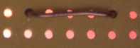
 file There is a wiring error somewhere, or there is a short circuit. Check your wiring, and look for solder bridges or any other kind of short circuit. Also, examine the connector for damage, or bits of metal dropped inside, and check to see if the ROM is inserted correctly.
    Copied ROM looks fairly OK -- it resembles a standard .BIN ROM file, although it won't run under the emulator. The problem could be slight damage to the ROM, an emulator problem, a file format problem, or a checksum problem. Do all the things for an intermittent fault -- it may be slightly damaged, so try copying slower, and checking your wiring. More importantly, make sure you used the .BIN file extension to save the ROM -- if you call it .SMD then it won't read properly. Also, try doing a FIX CHECKSUM on the emulator, and trying different emulators, as well as playing around with the options. It may be that the ROM simply won't work under the emulators.


    END OF FILE