I was going to make my next big post on how microinstructions are addressed and encoded, but before that I decided it was important to start with a primer on understanding the CPU schematic diagrams. It's taken longer than I thought to write this part up, so I'm going to post it now and cover the 68000 microinstructions sometime in the next few days.
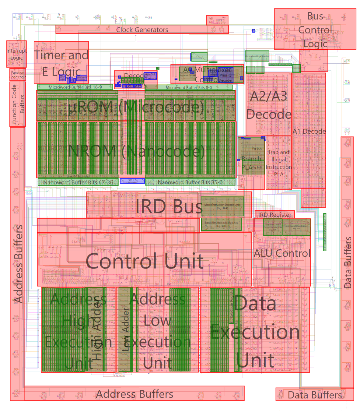
I've updated my Schematic Explorer with numerous bug fixes. I've also pushed an update to the schematic annotations, adding a lot of comments and annotations around the areas relating to microinstructions in particular, with some references back to the patent documents. Here's an overview of how it's looking right now:
If you want to understand the things I'm talking about in detail, I'd strongly suggest downloading Schematic Explorer and the annotated schematic so you can view the areas I'm talking about and follow along.
You can download the latest Schematic Explorer build here:
http://nemesis.exodusemulator.com/M6800 ... rerV1.4.7z (
github)
And you can download the annotated schematic from the github repo here:
https://github.com/RogerSanders/M68000Schematic
Interpreting die photos
In the questions/posts above, some basic coverage has been given on examining the raw die images and identifying transistors and connections on the die. I won't cover that in any more detail, and will instead focus on the schematic that Olivier has generated from the analysis of the die shots. While being able to refer back to the die shots is important in order to be able to double-check the schematic, tracing data flow and decoding logic from the die shots alone is much more difficult, and isn't practical to do for large regions. Generating a schematic is really a vital step in order to properly understand and document the internal workings of a device with this level of complexity. If you want to understand more about this essential first step of the process, review some of the posts prior to this one. The output from die shot analysis should be a series of masks representing each layer and the locations of vias connecting them (which can be generated from a vectorized image, as is the case with the analysis Olivier has done), from which a schematic can be generated through software analysis.
Interpreting the schematic
In order to follow what comes next, it's important to be able to understand the die schematic. There's really only one thing on the schematic we care about for the digital operation of the chip, and that's the MOSFETs and the connections between them. You may think a CPU is built from logic gates, and you may have heard that you can build any kind of logic circuit from a NAND gate. While that's true, gate structures like NAND gates don't exist as complete, discrete components on the die. These logic elements, as well as lots of other logic that doesn't fit the mold of traditional gates, are all built by a single underlying element, the MOSFET. MOSFET stands for "metal–oxide–semiconductor field-effect transistor", or "fet" for a shorter (technically not 100% equivalent) term. This is really the only kind of transistor that exists on the die surface. This is what we're measuring when we're counting transistors in a chip.
What is a MOSFET
I'm not going to fully discuss the design of a MOSFET, its variations of fabrication and usage, and so on here. There's more than enough written on the internet on this subject elsewhere which can be referred to if you want to know more. The Motorola 68000 being discussed here was fabricated using HMOS fabrication, which is a slight improvement over NMOS fabrication, and uses N-channel MOSFETs in both enhancement and depletion mode. Researching those terms will lead to more complete references on the subject. To understand the 68000 schematic, we simply need to understand that a MOSFET can serve two main roles:
1. As a digital switch
2. As a resistor
We'll cover both uses below.
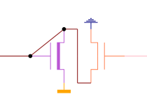
A MOSFET as a digital switch
This is the most important function of the MOSFET in digital electronics. Here's a picture of a MOSFET operating as a switch
In a nutshell, we have the "gate" terminal coming in at the top, with "source" on the left and "drain" on the right. If there's a voltage applied to the gate terminal (IE, logic level 1), then the switch is open, and the source and drain terminals conduct. Power can flow either direction through the source and drain terminals, for our purposes they're equivalent. No power flows from the gate to either the source or the drain, but having it sitting at a high logic level will connect the other two terminals together.
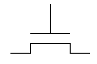
A MOSFET as a resistor
This is a MOSFET operating as a resistor:
This is a depletion-mode MOSFET, which in the case of the 68000 (at least in this schematic) seem to operate in a permanently open state. The MOSFETs in this case, as I understand it, are purely there to provide some resistance (load) between a power source and the rest of the circuit. You will usually (always?) find these fets attached to the +5 volt rail, which is represented here by the bar connected to the left. With the switch permanently open, and the gate also tied to the output, this is basically tying all three connecting lines together, so what's the point of it? As I understand it, without some kind of resistance in the circuit, where there was a connection between +5v and GND, too much current would flow, causing significant power draw and heat generation. The MOSFETs here are simply to limit the current flow, and if this was an external circuit rather than an integrated one, resistors would probably take their place. Fabricating them out of MOSFETs on the die surface however is more efficient. For all intensive purposes however, when we're only interested in the digital operation of the chip, when we see one of these MOSFETs in the schematic we can just consider them to be a permanent connection between whatever's coming in on all three terminals.
Building gates from MOSFETs
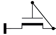
Putting it together now, here's a look at how logic gates can be built. Here's a simple NOT gate:
In this case, the line on the right is the input, and the line on the left is the output. The depletion-mode fet on the left is always open, so it will be pushing the logic level to high on the output line, unless the input line is high. In this case, the fet on the right will open, connecting the depletion-mode fet to gnd. Since the input current is limited by the depletion-mode fet, the line will be easily pulled to gnd, and since the gate of the depletion mode fet is tied to the output too, the output line will also be pulled low. Effectively anytime you create a connection to gnd, anything connected to that point, including through open fets, will be sucked down to logic level 0.
Let's take a look at something a bit more involved:
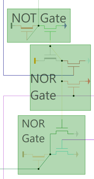
Here we have a portion of the group 0 exception handling logic, with some classic gate structures identified. We have three inputs. The blue and purple lines coming in from the top and bottom and tied to the inputs at the central NOR gate signal when a bus error or an address error is being asserted, respectively. If either of these inputs are true, the central NOR gate will change state from 1 to 0. Note that if the two inputs were connected through two fets in series rather than in parallel, we'd have an AND condition here rather than an OR condition. Above this, the NOT gate will flip the result to drive the output leaving from the top center, effectively making that a simple OR result of whether an address or bus error is currently being asserted. At the lower right, we have another line coming in representing whether a reset, bus error, or address error exception is currently being processed. This is combined with the NOR output from the the section above as the inputs to another NOR gate. The output from this would be a 1 if there wasn't an address or bus error active, and there wasn't currently a reset, bus error, or address error exception being processed, or at least that would be the case, if the input coming in at the lower right was active high, but it's not, it's active low. As a result, the output will only be 1 if an address or bus error is raised while one of those listed exceptions is being executed. This is the logic that detects a double bus fault condition, as described in the 68000 Users Manual section 6.3.9.1.
If that sounds complicated, break it down to smaller pieces. A single fet is easy to understand by itself. If you can understand the signal that's driving it, you can look down at the effect it will have on the fets that it connects to, and so on. If you can't figure out what's an input vs an output line, pay attention to the gate terminals. Remember that the gate terminal on a fet can't pass any output current, it can only be fed an input, so anytime you come across a line being fed directly into a gate, as long as it's not the gate for a depletion-mode fet with a connection back to the gate, you know that line is being driven as an input.
Building Latches from MOSFETs
One more important aspect of the use of MOSFETs is how they can be combined to store data. A circuit to do that is called a flip-flop or a latch. Diving right in, here's a real example from the 68000 schematic:
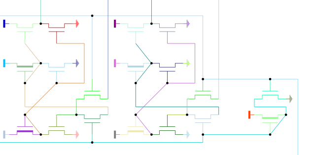
Here we have latches for two bits, in this case for bits 9 and 8 of the latched A1 microcode address. You should be able to see these two "cells" as mostly identical blocks forming most of this image. Leaving from the top center of each "cell" are the output lines from the bit latches, which are either high or low depending on what the currently stored value is in each latch. Coming in from the top down into the right side of each cell are the input data lines, which are used to feed a new value into the latch to store. Coming in from the bottom then across from the right we have a control line, which is asserted to open the latches and capture the current state of the input data lines. This control line has its logical NOT state computed to form a second control line, which will always be the opposite logic level of the other. These two control lines run to each cell.
Now looking at the operation, inside each cell there are two depletion-mode fets actively trying to drive the circuit. When the latch is open to capture the input state, the input line directly drives the gate of a fet in the bottom center of each cell, which will control whether the bottom depletion-mode fet is grounded or not. If that fet isn't grounded (IE, input is 0), it will ground the depletion mode fet above it, and it will ground the output line state too. If that fet is grounded (IE, input is 1), the fet above it will drive the output line to true. In both cases, the output of the middle depletion mode fet will also try and drive the ground state of the lower fet too, but it's currently disconnected from the gate by the control line state. Note that the depletion mode fet in the middle mirrors the logic state of the input line when the latch is open. When the latch is shut, the input line is disconnected, but at the same time the output state from the depletion mode fet in the middle, which was mirroring the input line state, is connected in its place. Since that fet was forced to mirror the logic state of the input line, when the lines switch over, it will take the place of the input line and hold the latch in the same condition continuously from that point forward, until the control signal switches again and feeds a new value on the input line.
Latches can be built in different ways, but this shows the concept and a specific case of latches being used in the 68000 processor. To recognize latches, look for logic blocks where two depletion-mode MOSFETs can control the ground state of each other.
Inverting and non-inverting superbuffers
A quick word about superbuffers. Superbuffers are (of course) build from MOSFETs, but unlike the logical elements described above, their purpose is more in the analog domain. If you have a single line that needs to drive the gate inputs to many fets, it needs to have a nice, strong power source. If you need to give a line a little more oomph, throwing in a superbuffer is a bit like an amplifier, boosting the signal (ehhh, maybe not really, but you get the idea). Superbuffers come in two primary forms, inverting and non-inverting. Here they both are:
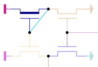
Inverting superbuffer
Non-inverting superbuffer
Now note that as ijor pointed out in a previous post, the schematics are actually incorrect here. Both the fets tied to +5v here are the depletion-mode type, and the non-inverting superbuffer is a little more complex in the way its connected I believe, but for understanding the logical operation of the processor none of this is important. A non-inverting superbuffer, from a logical perspective, makes absolutely no difference to the circuit. Logic level high comes out as high, and low comes out as low. An inverting superbuffer does affect the result however, as it acts as a NOT gate, so high comes out as low and vice versa. Superbuffers are commonly used as drivers on reasonably sized PLA structures, which is a nice segway into the next section.
PLA Structures
PLAs make up a big part of the overall die space, most of it related to microinstructions, so you need to understand them. PLA stands for Programmable Logic Array, and you can read up on them separately if you want. To give a brief overview, I'm going to borrow (read: steal) a diagram on PLAs from the 68000 patent documents:
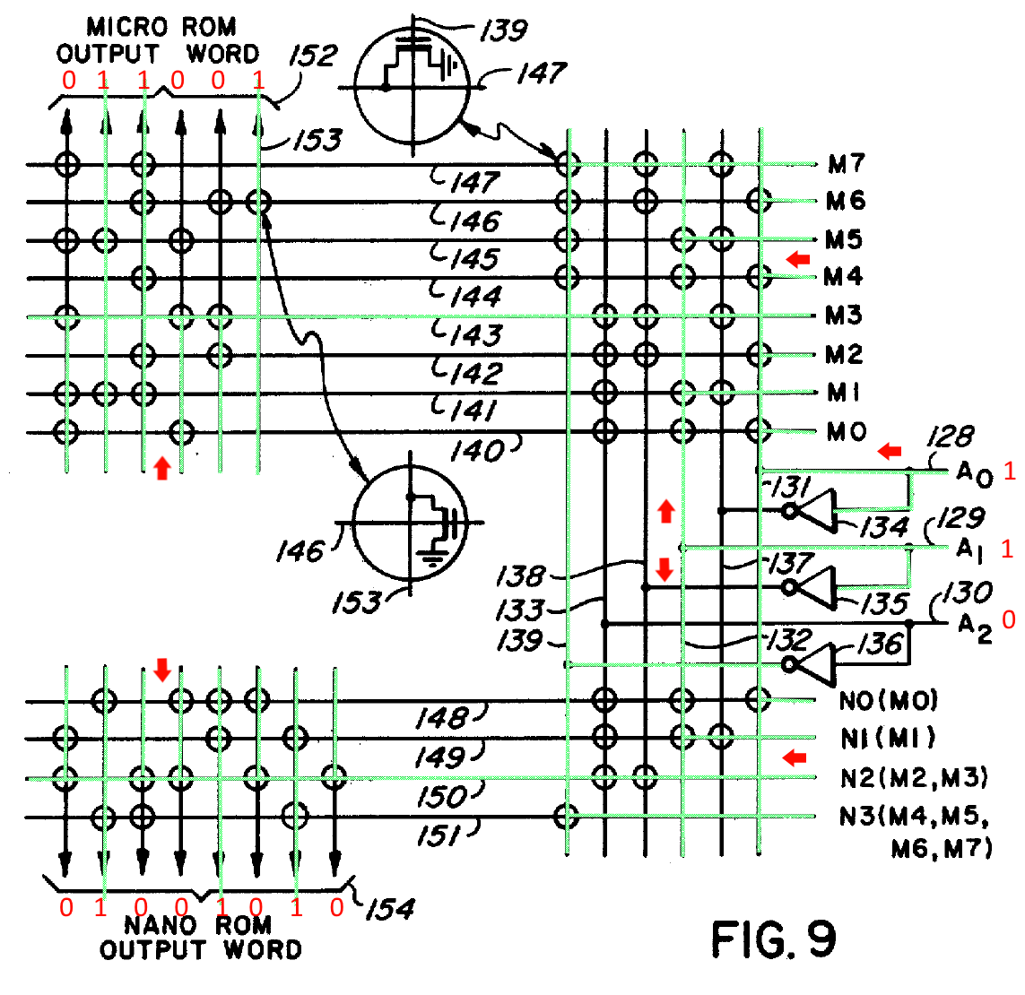
This maybe isn't the best showcase of PLA design, but I had it on-hand. The arrows here show the direction of our theoretical "positive charge flow", with the traces marked in green showing where our charges are notionally flowing. The basic concept is simple: you feed a value in, and you get at least one value out. In this way it's just like an array, or lookup table if you will. The image above actually shows two separate values being returned from a single lookup. Some PLAs in the 68000 are like this, but basic PLAs are just map a single input value to a single corresponding output value. The nice thing about PLAs is that where you have redundant data, IE, two separate input values produce the same output value, it's often possible to shrink the size of the array logic and "key" that shared output value to respond to two (or more) inputs, if your input values are cleverly chosen.
Here's how the basic PLA works. Lets say you have a 3-bit input value, as shown in this example. You feed in those three separate lines, and their compliments (inverse/logical NOT) into the array, so for a 3-bit input we have 6 lines. Those lines drive our "rows" in the PLA (shown vertically here). Running perpendicular to the rows are our column lines. In the image, you should be able to recognise the presence of fets. In this case, the small circles present on some of the line intersections represent the presence of a fet. Where a fet is placed between a row and a column, with the row activating the gate on the fet, it ties the column line to ground. The columns are all fed with a +5v source. In a traditional well-formed PLA, one column line, and only one, will remain active for any given input. You place the fets to eliminate the columns that can't match based on the input line state, until only one remains, which selects the desired output value. Where you want a column to activate when a given input bit is set to false, you place a fet on the row that carries that input bit, so that it'll be ruled out if that bit is true. If you want a column to activate when an input bit is true, you place a fet on the compliment of that line, so that it'll be ruled out if it's false. If you don't care what the state of a given line is, you don't place a fet on either line. You can think of this as a combination of a matching value with a bitmask, or a target value with wildcards (IE, value 0b1100 mask 0b1110, or 110?, to match 0xC/0xD). Once the column is selected, it runs into another grid, this time as the row, where again +5v is driving all the column lines. The column lines here represent your output data. At this point, you simply place fets on the column to ground the column the bits you want to set to 0 for each entry in your table, and leave the ones you want set to 1 to pass straight through.
I'm going to leave things there for tonight. I think this is enough of a primer on the schematic itself. Next big post will cover microinstruction addressing and decoding.
 . Looks like the buried contacts must take a fair bit of squinting to pick up in all cases too. The gradient on the edges in the third delayer pick gives it away fairly well though. I suppose we're lucky it's possible to figure out these things by eye at all.
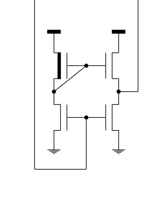

