I'm officially building a microcode-level 68000 core
Moderator: BigEvilCorporation
Re: I'm officially building a microcode-level 68000 core
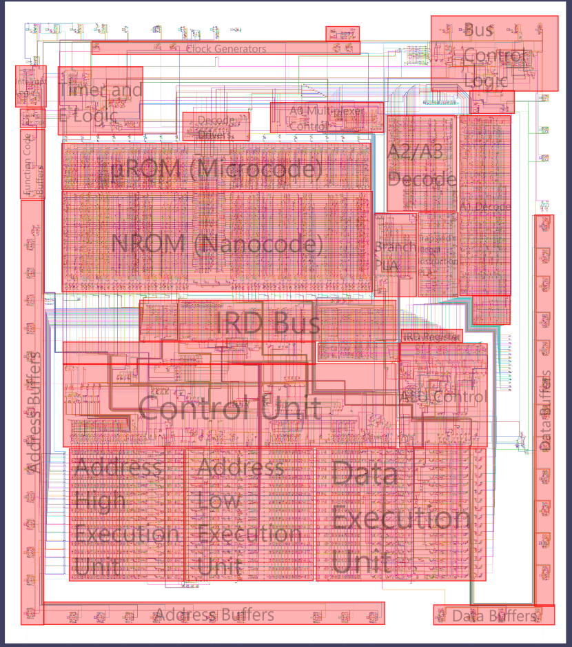
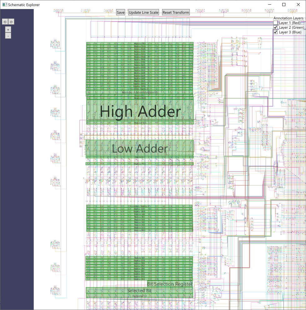
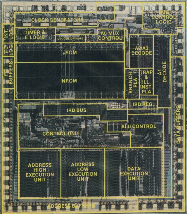
I've done another quick update to the schematic explorer. I've also completed a quick initial transfer of the annotations from the "official" die layout. Here's the original image:
This was provided by Motorola about a billion years ago. It shows an ultra low-res shot of the 68000 die, with some major processing "blocks" defined.
Here's how it appears in the schematic view:
It looks a bit nicer when you're zooming in and scrolling around, seems a bit "dead" in an image. I haven't done any "sanity checking" of this, it's just a quick 5 minute job, but it serves as a useful starting point for analysis.
You can download the schematic with the attached annotation layer here: http://nemesis.exodusemulator.com/M6800 ... otated1.7z
Just load it into the schematic explorer, which you can download here: http://nemesis.exodusemulator.com/M6800 ... rerV1.2.7z
Re: I'm officially building a microcode-level 68000 core
Looking forward to your work, Nemesis. I’m actually going to be starting on my own 68K HDL project for a personal project. If I find anything I’ll let you know. I’ve tinkered with the idea of taking the schematic you’ve posted and the text description of it and writing an program that searches for logic gates and reduces the transistors to their logical equivalents. If I make any headway I’ll post the info here.
Re: I'm officially building a microcode-level 68000 core
I've had a crack at annotating the physical location of the internal registers on another layer:
This is primarily based on the work Gigasoft did, and I've used the register names he used. The annotation it isn't complete, as I got a bit lost in the ALU. There could also be errors, so feedback and corrections are welcomed. The names of internal registers will need correcting, once we've confirmed the proper names for each one from the patents. If anyone who's done more work on the physical layout wanted to take a look at this and expand on it, it'd be very much appreciated.
Here's the updated schematic:
http://nemesis.exodusemulator.com/M6800 ... otated2.7z
And here's a new version of the schematic explorer, which fixes some hit testing issues: http://nemesis.exodusemulator.com/M6800 ... rerV1.3.7z (source)
Re: I'm officially building a microcode-level 68000 core
That'd be awesome, I think that would make it a lot more accessible. I sunk hours yesterday into trying to get some understanding on HMOS gate design. Plenty of the IC layout still prompts a lot of "...WTF?" responses when I look at it.Enforcer wrote: ↑Wed May 15, 2019 4:51 amLooking forward to your work, Nemesis. I’m actually going to be starting on my own 68K HDL project for a personal project. If I find anything I’ll let you know. I’ve tinkered with the idea of taking the schematic you’ve posted and the text description of it and writing an program that searches for logic gates and reduces the transistors to their logical equivalents. If I make any headway I’ll post the info here.
Re: I'm officially building a microcode-level 68000 core
I've created repos on GitHub for Schematic Explorer and the Annotated 68000 Schematic. If anyone wants to contribute, just fork the repo and submit a pull request.
Re: I'm officially building a microcode-level 68000 core
*taptaptap* is this on? Damn there's so much dust in this account.
The schematics are made from the hand-made vectorization at https://og.kervella.org/m68k/layers.svg
The metal layer was done by quietust, everything else by me.
You then need to grab and compile my dietools (https://github.com/galibert/dietools, they even compile and work on windows thanks to cr1901). Run generate.sh (from kervella) and after eating way too much memory and disk space you get a bunch of files. You can then run mview mv-config.txt to see the result of the vectorization extraction. It also include a simulator that doesn't work.
Then you run sgen/remap.lua and you get a beautiful schem.txt you can see with sview schem.txt. sview allows you to see the schematic, select signals, and see the names I've given the circuits I understood. It also includes a different simulator that doesn't work either.
None of these tools are nice to use. They're not documented, and frankly they've been built following my needs. If you submit PRs, I'll probably accept them. If you send me an email telling me "I have done something, are you interested?" there's a 50% chance I think "sure" then forget to answer (yes, it has happened already).
To be honest, if you can't manage to build them and use them for the m68k by yourself, you may not be proficient enough to use that undocumented, undesigned, somewhat badly structured mess.
Re: I'm officially building a microcode-level 68000 core
Answering some questions from Nemesis in another place.
What is the quality of the schematics? Very high. They've already been used once to build a perfect fpga 68k core. No, not ijor. No, I won't say by who, he or she can talk about it if he/she wants to. I've got a ton of information back, I just didn't have to time to use it all at the time. But I'm fairly certain I can ask for more once I get back to working on that core. I still have some refactoring to do in the current mame core before it's sane.
Is everything in the micro/nanocode? Not at all, by far. There are roughly 200 control signals to the EU, the registers, etc. There are more or less 70 signals coming from the micro or nanocode (68 from nano plus the two bus access type from micro). the 70->200 expansion is controlled by a ton of PLAs keyed on the IRD register. Plus other things are fully PLAd, like the exception/interrupt vector addresses.
The tech is HMOS, which means high-density NMOS. A NMOS enhacement mosfet conducts on gate 1 and doesn't on 0. A NMOS depletion mosfet (the black ones) always conducts, it's pretty much a pull (up or down depending on what's on the other side), and the gate doesn't really matter. A normal NMOS gate (68000 does normality only up to a point) has a bunch of enhancement mosfets connecting the output to gnd, and one depletion pulling to one.
Whoever wondered about bool x = !(a || b || c || d || (e && f));, well, that's a nmos structure.
Re: I'm officially building a microcode-level 68000 core
Hey thanks for (re)joining us!galibert wrote: ↑Thu May 16, 2019 6:07 pmThen you run sgen/remap.lua and you get a beautiful schem.txt you can see with sview schem.txt. sview allows you to see the schematic, select signals, and see the names I've given the circuits I understood. It also includes a different simulator that doesn't work either.
Just last week I tried doing exactly this. I installed cygwin, built dietools, built the pbm's, built the layers.map/svg, then tried to run sgen/remap.lua but unfortunately got this:
Code: Select all
Error: megabus.lua:103: attempt to index a nil value (local 'nl')
Code: Select all
Error: megabus.lua:1671: bad argument #1 to 'move' (node hash expected)
Re: I'm officially building a microcode-level 68000 core
Ah, have you pushed to the dietools github? Last commit was 11 months ago
Re: I'm officially building a microcode-level 68000 core
I *think* that was technically up-to-date, but I synced with my current experiments just in case (they don't matter if you don't use the new functionality, otherwise they don't work iirc
OG.
Re: I'm officially building a microcode-level 68000 core
Thanks heaps. I'll have a shot at building those tools tomorrow. I like to make things hard for myself and build all this stuff on Windows.
So to confirm, the layers.svg file really contains all the important information, and it was manually created by yourself and quietust by tracing from the die shots. Everything from there, like the schematic and the decoded PLA data, comes from tool analysis from the layer information. That sound about right? One thing I'm not clear on is how exactly do you identify the transistors from the layer information alone. This is probably obvious to some people, but I'm not "getting it" right now. I thought I was figuring it out, but it's not tracking with your schematic, and I haven't come across a good description online about this. I can (and will) tear apart your code soon, but could you elaborate a bit on this aspect? I really want to understand this process top to bottom and document it.
Let me focus on a specific example. Take this region, where the IRD register contents have inverted lines generated and are fed into the A1 decode PLA:
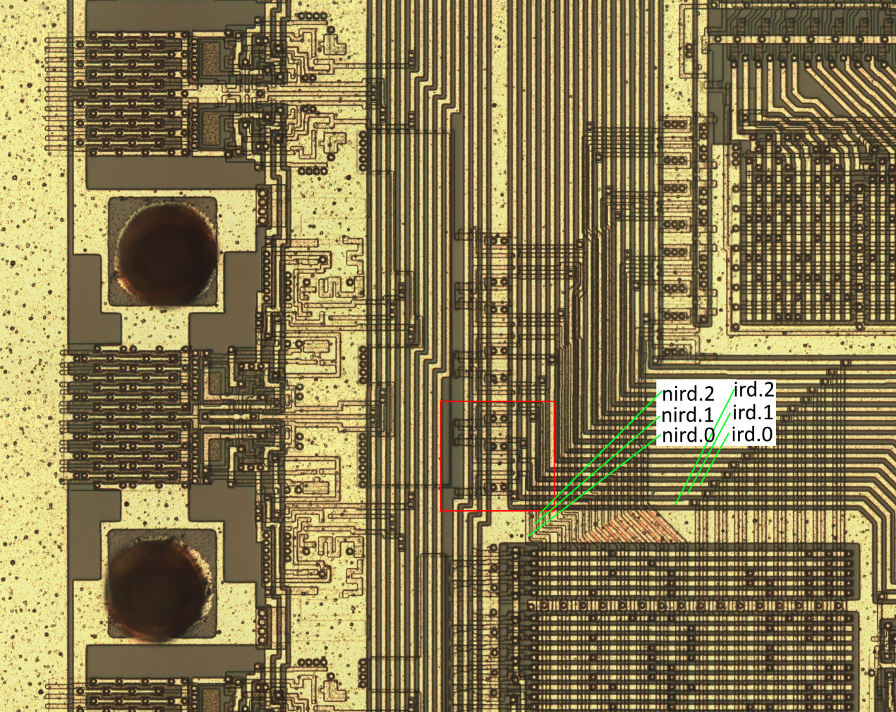
I've annotated the lower three bit lines here, using the same line names you use in your schematic. If I'm following this right, the actual IRD contents are stored to the right of this (but I could be wrong), and this region is simply calculating the logical NOT state of the IRD lines.
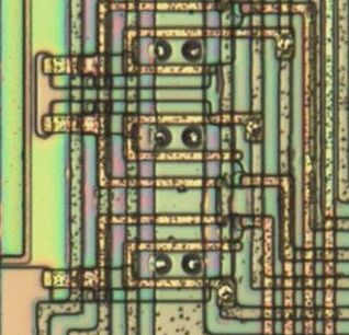
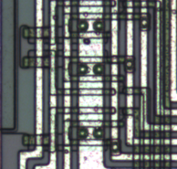
Here's a close-up of the specific region from the original visual6502 decap (containing ird/nird 0-2):
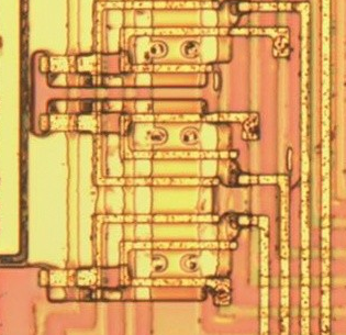
Here's the same region from the newer decap:
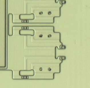
And here's the region again from layers.svg:
Although I can see how you visually isolate the layers from these images, (which must have truly been a tedious, time-consuming process, so props for doing it!), I don't think I'm properly understanding how you determine the actual transistor logic from what's in front of me. For a single bit line in this region, here's what you show in your schematic:
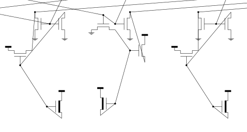
Here we see ird.0 coming in down the left then up from the bottom, and nird.0 going out on the right. Since your clarification about HMOS fabrication (thanks for that) this is making more sense. Based on your description, I assume the MOSFET here with the thick line on top is a depletion fet, which if it's always open acting as a pullup as you described, this logic functions as I'd expect. The ird.0 line is routed to the gate of the two lower enhancement mode MOSFETs, grounding them when ird.0 is true, which forces nird.0 to false. When ird.0 is false, the gates are closed, leaving the pull-up fet to lift the gate of the fet on the top right, which without grounding ties nird.0 to +5v setting it to true. That makes perfect sense. How do you get from a visual inspection of the layers shown above though, to this schematic?
Another question too, in terms of the die shots themselves, where did they come from? I know you said in the past the ones from the visual6502 guys weren't high resolution enough. You've got a series of four higher resolution die shots from decapping through stages of delayering. Did you arrange those ones yourself, or do they come from some other source? Not really important from a technical perspective, I'm just curious.
So to confirm, the layers.svg file really contains all the important information, and it was manually created by yourself and quietust by tracing from the die shots. Everything from there, like the schematic and the decoded PLA data, comes from tool analysis from the layer information. That sound about right? One thing I'm not clear on is how exactly do you identify the transistors from the layer information alone. This is probably obvious to some people, but I'm not "getting it" right now. I thought I was figuring it out, but it's not tracking with your schematic, and I haven't come across a good description online about this. I can (and will) tear apart your code soon, but could you elaborate a bit on this aspect? I really want to understand this process top to bottom and document it.
Let me focus on a specific example. Take this region, where the IRD register contents have inverted lines generated and are fed into the A1 decode PLA:
I've annotated the lower three bit lines here, using the same line names you use in your schematic. If I'm following this right, the actual IRD contents are stored to the right of this (but I could be wrong), and this region is simply calculating the logical NOT state of the IRD lines.
Here's a close-up of the specific region from the original visual6502 decap (containing ird/nird 0-2):
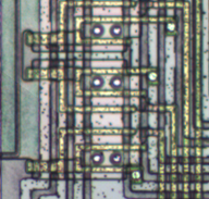
Here's the same region from the newer decap:
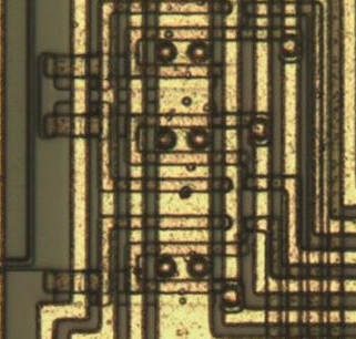
And here's the region again from layers.svg:
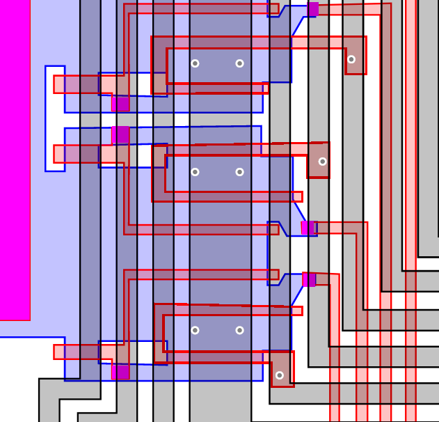
Although I can see how you visually isolate the layers from these images, (which must have truly been a tedious, time-consuming process, so props for doing it!), I don't think I'm properly understanding how you determine the actual transistor logic from what's in front of me. For a single bit line in this region, here's what you show in your schematic:
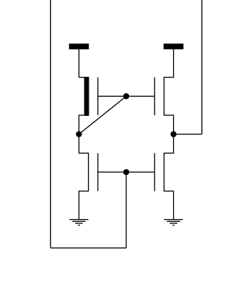
Here we see ird.0 coming in down the left then up from the bottom, and nird.0 going out on the right. Since your clarification about HMOS fabrication (thanks for that) this is making more sense. Based on your description, I assume the MOSFET here with the thick line on top is a depletion fet, which if it's always open acting as a pullup as you described, this logic functions as I'd expect. The ird.0 line is routed to the gate of the two lower enhancement mode MOSFETs, grounding them when ird.0 is true, which forces nird.0 to false. When ird.0 is false, the gates are closed, leaving the pull-up fet to lift the gate of the fet on the top right, which without grounding ties nird.0 to +5v setting it to true. That makes perfect sense. How do you get from a visual inspection of the layers shown above though, to this schematic?
Another question too, in terms of the die shots themselves, where did they come from? I know you said in the past the ones from the visual6502 guys weren't high resolution enough. You've got a series of four higher resolution die shots from decapping through stages of delayering. Did you arrange those ones yourself, or do they come from some other source? Not really important from a technical perspective, I'm just curious.
Re: I'm officially building a microcode-level 68000 core
The ton of lua in sgen moves things around to make the schematic more readable (and fixes a small number of depletion/enhancement errors). You can see the raw extraction in the just added schem-non.svg
The region you're showing (could you orient your die shots the way I have the schmatic please?) looks like that uncleaned:
You can see the group of 4 transistors in their real position. In the layers, blue is active (bottom layer), red is polysilicon (just on top of it), black is metal (on top of it all), pink is buried contacts (connections between action and poly), circles are vias (connections between metal and poly or active), elsewhere green is capacitors (between active and poly).
A transistor is where poly is over active and it's not something else (e.g. not buried or caps). The gate is the poly, and the terminals are the active on both sides of the poly. You thus can easily see the four transistors, and you can guess that the buried on the left goes to +5V and the large metal in the middle with the vias goes to ground. Depletion and enhancement aren't visually distinguishible, but my tools have heuristics to decide (correct at 99.99% or so, which ain't bad).
Then the lua code moves things around to make such an inverting amplifier more readable.
The origin of the die shots is http://siliconpr0n.org/map/motorola/mc68000p8_a72e/. They're been done at my request but not by me I've rotated and aligned them for my use, you have the result on kervella. Not sure why I rotated them, probably to orient the text correctly, but after several years working on them I have my habits.
Re: I'm officially building a microcode-level 68000 core
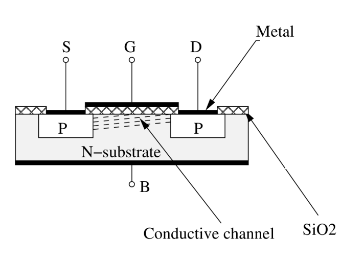
I think I'm starting to get it. Here's a cross-section of an N-channel MOSFET for reference:
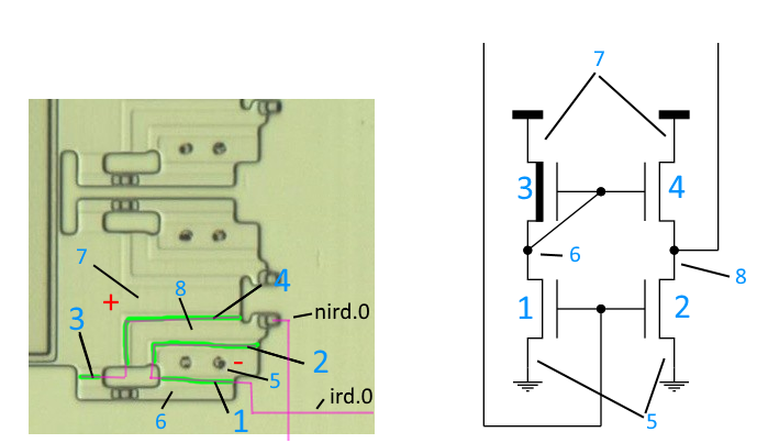
The gate is defined by an insulated trace that runs over the top of the substrate. With an enhancement mode mosfet, when it's active power will flow through the substrate underneath it, connecting the two regions on either side. Importantly, the fets can be any length, they're really just an arbitrary "stripe" along the surface that can be laid down pretty much however you want, within the limits of the fabrication process. In the images above, the final of the four new decap pictures clearly shows the region of the circuit where... well I'm not sure exactly yet, I'll need to research more. Is this where the n-substrate is laid down, or just where it isn't insulated in some manner? At any rate, it effectively shows the region in which transistors can be formed. Where the "gate" traces run effectively define the MOSFETs. For the "standard" enhancement mode fets, the two regions immediately on either side of the gate trace will be bridged when current is flowing through the gate trace. Here's a breakdown of the area I raised above, mapping to the schematic:
The areas marked in green are where the MOSFETs are formed, by the presence of a gate track running over them. The path the tracks take are shown in pink. The numbers correlate each gate, and each source and drain connecting to them, between the die surface and the ones in the schematic. Tracing the metal layer shows the connections between vcc and gnd, which have been stripped from this image but can be correlated in other die shots, to determine which parts of the substrate are tied to ground, +5v, or left indeterminite/floating, in this case leaving them free to be pulled high or low by the MOSFETs.
Re: I'm officially building a microcode-level 68000 core
Ahhh, just saw your reply! Took me an age to do the image work on my post. I'm reading through yours now and comparing to what I came up with, let me see if I was on the right track....