I have a question about M68000 input signals.
For example IPL0, IPL1 ...
Imagine that you set IPL0 and you unset it before the end of the current opcode.
The interrupt will be cancelled?
Thame thing for BUSREQ and other input signals.
About M68000 signals
-
Chilly Willy
- Very interested
- Posts: 2984
- Joined: Fri Aug 17, 2007 9:33 pm
That's all described in the manual, which is available online for free. You can find it darn near anywhere. I suggest you read it. It also gives you the timings for instructions, and info the number of read and write cycles done per instruction.
The bus section described all the signals, as well as the timings for hold on signals before they are considered valid.
Just google for it.
The bus section described all the signals, as well as the timings for hold on signals before they are considered valid.
Just google for it.
-
HardWareMan
- Very interested
- Posts: 745
- Joined: Sat Dec 15, 2007 7:49 am
- Location: Kazakhstan, Pavlodar
-
Chilly Willy
- Very interested
- Posts: 2984
- Joined: Fri Aug 17, 2007 9:33 pm
Yeah. Motorola published one programming reference for the "family", and then user manuals for each individual chip that covered the hardware and any differences to the main spec. So you'll find user manuals for the 68000, 68020, 68030, 68851, etc, but just one Programming Environment Manual covering all aspects of programming the 680x0 family processors.HardWareMan wrote:I just clarified: See M68000 User Manual. Because there is M68000 Programmers Manual, where signals and timings are not described.
-
HardWareMan
- Very interested
- Posts: 745
- Joined: Sat Dec 15, 2007 7:49 am
- Location: Kazakhstan, Pavlodar
Here. Also, I know that 190ns ROM works very unstable (I guess ROM must be quicker than 110ns).mickagame wrote:Does the latency of ram/rom has been measured on real sega genesis?
-
Chilly Willy
- Very interested
- Posts: 2984
- Joined: Fri Aug 17, 2007 9:33 pm
It doesn't run slow - the Genesis uses a "standard" DTACK timing that is either met by roms, or isn't. Roms that meet the timing all work the same - roms that don't will crash when data isn't read correctly due to too fast timing on the DTACK. The Genesis is not capable of changing the timing of the DTACK for carts. If a cart needed special timing, it would have to use an address space where the Genesis doesn't assert the DTACK, then generate its own DTACK with the proper timing. No one does that.
-
HardWareMan
- Very interested
- Posts: 745
- Joined: Sat Dec 15, 2007 7:49 am
- Location: Kazakhstan, Pavlodar
Right. According to this picture:Chilly Willy wrote:It doesn't run slow - the Genesis uses a "standard" DTACK timing that is either met by roms, or isn't. Roms that meet the timing all work the same - roms that don't will crash when data isn't read correctly due to too fast timing on the DTACK. The Genesis is not capable of changing the timing of the DTACK for carts. If a cart needed special timing, it would have to use an address space where the Genesis doesn't assert the DTACK, then generate its own DTACK with the proper timing. No one does that.
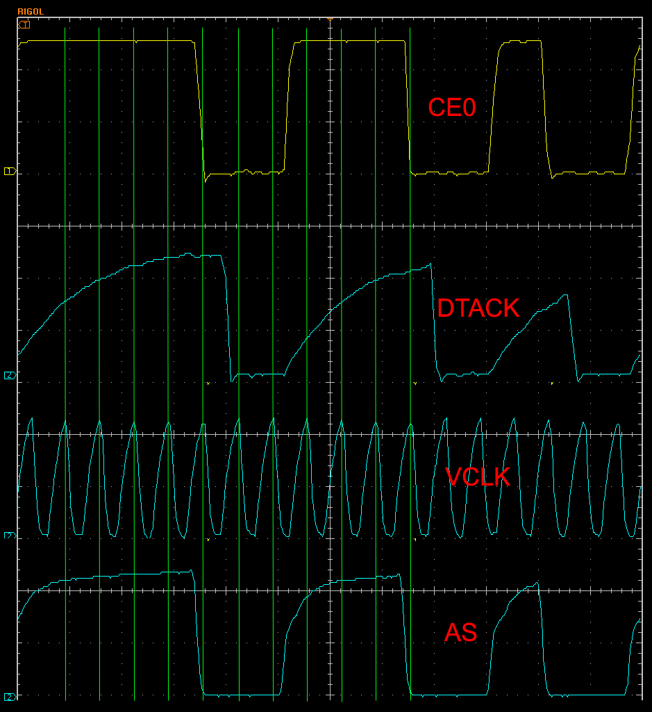
According to M68000UM:
This is fastest possible DTACK negotiation for M68000.M68000UM wrote:STATE 0 The read cycle starts in state 0 (S0). The processor places valid function codes on FC0–FC2 and drives R/W high to identify a read cycle.
STATE 1 Entering state 1 (S1), the processor drives a valid address on the address bus.
STATE 2 On the rising edge of state 2 (S2), the processor asserts AS and UDS, LDS, or DS.
STATE 3 During state 3 (S3), no bus signals are altered.
STATE 4 During state 4 (S4), the processor waits for a cycle termination signal (DTACK or BERR) or VPA, an M6800 peripheral signal. When VPA is asserted during S4, the cycle becomes a peripheral cycle (refer to Appendix B M6800 Peripheral Interface). If neither termination signal is asserted before the falling edge at the end of S4, the processor inserts wait states (full clock cycles) until either DTACK or BERR is asserted.
STATE 5 During state 5 (S5), no bus signals are altered.
STATE 6 During state 6 (S6), data from the device is driven onto the data bus.
STATE 7 On the falling edge of the clock entering state 7 (S7), the processor latches data from the addressed device and negates AS, UDS, and LDS. At the rising edge of S7, the processor places the address bus in the highimpedance state. The device negates DTACK or BERR at this time.