I meant the SCU DSP not the SCSP DSP. It was meant to be a vector coprocessor apparently, but it was woefully inadequate in many ways - including, but not limited to, documentation.
Sonic Jam used streaming ADPCM for the music, and normal PCM for most of the sound effects. One or two sound effects MAY have used FM in them, it was used in a scarce way like that in many, many games.
New Documentation: An authoritative reference on the YM2612
Moderator: BigEvilCorporation
-
TmEE co.(TM)
- Very interested
- Posts: 2440
- Joined: Tue Dec 05, 2006 1:37 pm
- Location: Estonia, Rapla City
- Contact:
SCU has maaany of pages of documentation. I went through my saturn docs to find some SCSP info and I came accross with at least 10x PDFs full of SCU stuff. Only few that dealth with SCSP, and from those few, SCSP DSP had no meaningful info.
Mida sa loed ? Nagunii aru ei saa 
http://www.tmeeco.eu
Files of all broken links and images of mine are found here : http://www.tmeeco.eu/FileDen
http://www.tmeeco.eu
Files of all broken links and images of mine are found here : http://www.tmeeco.eu/FileDen
-
Stef
- Very interested
- Posts: 3131
- Joined: Thu Nov 30, 2006 9:46 pm
- Location: France - Sevres
- Contact:
Maybe things changed with time because indeed the SCU DSP documentation was the most undocumented part sometime ago.
Hopefully that was not a big deal for emulation as only a bunch of game actually use it (i did some work on SSE emulator but it was quickly discontinued by lack of time and because of the messy internal structure).
Hopefully that was not a big deal for emulation as only a bunch of game actually use it (i did some work on SSE emulator but it was quickly discontinued by lack of time and because of the messy internal structure).
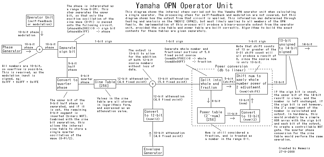
Just wondering, is anyone else trying to parse through the parts of the chip scan? I've been trying working through them, but my poor computer can't open the full scan without abusing the hard drive. So far I've identified the EG, PG, sine and exponential ROMs, sine/exp. output adder, etc., but actually figuring out the detailed functional parts and what goes specifically where is a lot more difficult, especially at lower resolution.
Anyway, I have to say, Nemesis' functional diagrams of the PG and the output section seem to be pretty spot on so far from what I've been seeing.
One thing may need to be done is to strip off the metal layer, to expose any hidden vias on the chip. It'll definitely make the chip itself nonfunctional, but the chip's guts will be completely scanned and could allow full vectorizing of the chip (and maybe even eventually a graphical simulation, like the 6502 and 6800 visual sims).
I haven't done any more analysis on it in quite awhile, I found it hard to identify elements from the die shot. It's good to hear you're making more progress. When you're able, maybe you could post an image of some of what you've identified, IE, a basic overlay identifying the main functional areas of the chip. I found it hard just figuring out the basics. I don't think I was even certain where the phase generator and envelope generator circuits were.
Stripping off the metal layer sounds interesting, I've seen some other die shots where that's been done, and it certainly seems to reveal more. I couldn't tell exactly from looking at the die shot what parts make up the metal layer. Do you believe doing that alone will be enough to reveal the entire internal structure of the chip?
Stripping off the metal layer sounds interesting, I've seen some other die shots where that's been done, and it certainly seems to reveal more. I couldn't tell exactly from looking at the die shot what parts make up the metal layer. Do you believe doing that alone will be enough to reveal the entire internal structure of the chip?
Here's the chip parts so far. (~500KB)
All of the sections in the top-left (not marked with a red box) are the various registers; I haven't yet figured which are which, but I'm going to assume the large and wide part in the middle-left are the main channel registers, and the smaller part in the very top-left are the misc registers (PCM data to Ch.6, LFO control, etc.). I've boxed off some of the other stuff elsewhere but I'm not completely sure what they are yet.
Basically, all the light yellow traces are metal (either aluminum or copper, depending on the chip). It's light yellow because the chip has a protective layer of silicon on the very top covering everything (it's also why some things may look wavy, distorted, or unclear). The metal layers may also reveal some of those hidden silicon features, since the metal is deposited over those features, the top of the chip will end up with valleys and hills everywhere. You may see some of those underlying features by the valleys and hills they form on the upper layers (in the big featureless metal areas), but usually they're concealed by the features above. Compare the various images of the 6502's layers here.
This is so cool. I got a noob question.. How do you know which part does what? How does one go about doing this?Momiji wrote:Here's the chip parts so far. (~500KB)
All of the sections in the top-left (not marked with a red box) are the various registers; I haven't yet figured which are which, but I'm going to assume the large and wide part in the middle-left are the main channel registers, and the smaller part in the very top-left are the misc registers (PCM data to Ch.6, LFO control, etc.). I've boxed off some of the other stuff elsewhere but I'm not completely sure what they are yet.
Basically, all the light yellow traces are metal (either aluminum or copper, depending on the chip). It's light yellow because the chip has a protective layer of silicon on the very top covering everything (it's also why some things may look wavy, distorted, or unclear). The metal layers may also reveal some of those hidden silicon features, since the metal is deposited over those features, the top of the chip will end up with valleys and hills everywhere. You may see some of those underlying features by the valleys and hills they form on the upper layers (in the big featureless metal areas), but usually they're concealed by the features above. Compare the various images of the 6502's layers here.
Mainly by looking at how many bits wide it is. For example, you can see the 10.10 bit wide registers in the PG, the 10 bit registers in the EG, the 14 bit output of the PG leading to the sine ROM, etc. Nemesis' PG-to-output and operator unit diagrams also helped figure out what goes where.Ricky wrote:This is so cool. I got a noob question.. How do you know which part does what? How does one go about doing this?
viewtopic.php?t=386&postdays=0&postorder=asc&start=476
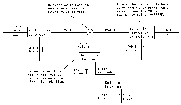
Indeed, if we take a look at how the phase increment table is calculated:
and how the 17-bit phase increment value is calculated from FNUM and BLOCK values:
we can see that:
1) the value is shifted for non-integer input/output samplerate ratio using 16.16 (FREQ_SH = 16) fixed point precision
2) the 10-bit right shift done by the chip on phase value (remember the size of phase counter is 20-bit, with lower 10-bit being dropped when calcultating the output) is actually "pre-included" in the returned increment value (the phase counter is later shifted by 16-bit instead to keep the needed precision samplerate ratio until then)
3) the BLOCK shifting done by the chip on FNUM value is taken account by returning a value already left-shifted by 6 (FNUM is multiplied by 2 to get an index between 2048-4095 in the table then by 32 out of the table) and then by righ-shifting the value returned by the table by 0-7, depending on BLOCK value.
Now, the flaws I potentially see with this design (please someone correct me if I'm wrong):
1) the 10-bit right-shift is done on the increment value instead of being done on the phase counter value itself -> actually, this is not really a problem because of the 6-bit (16-10) shifting added anyway so you don't lose the original 20-bit precision.
2) the added precision (6-bit) actually prevents the lowest FNUM bit to be dropped in case the BLOCK value is 0 -> this indeed actually increase the phase increment precision by one bit, for example if FNUM=0x01 and BLOCK=0, the phase counter will still be incremented on each cycle by (1 * 2 * 32 * (1 << 6)) >> 7 i.e 2048 (in MAME's core 16.16 fixed point precision) on each cycle while it should NOT have been updated.
I would appreciate any comment on this as I might indeed have missed something in the implementation.
Another unanswered question I have is about how LFO really works, how the phase and envelope modulation values are exactly calculated from PMS/AMS register values then evolving off course, but also how LFO unit works when it's being stopped or restarted.
The reason I ask is that an user reported me a sound issue with one track in California Games (the "Surfing event" track) and I kinda figured the problem was that the sound engine was continuously stopping/starting LFO to update each channel parameters and that it resulted in some channel (channel 3 specifically) to sound lower and differently pitched than it should.
I was initially resetting LFO modulation counter/values each time it was restarted and somehow got it to sound louder by leaving LFO state untouched when stopped/started but that's still not exactly pitched how it should and also inconsistent (got different result depending on when the track is restarted using the sound test).
I was thinking more about this recently and think I figured where the error in MAME core came from. It's not about the size of the table or added bit of precision for LFO (it's actually taken care of when calculating phase increment from 11-bit FNUM value, see below) but from the fixed point (16.16) precision that was added to make the chip run at other frequencies than the original one (i.e directly at the desired samplerate, without having to resample the output).Nemesis wrote:Not yet. Sorry, I've been really short on free time lately, so I've had to dial back on this stuff for a while. If you've got a specific question, I should be able to answer it. In terms of writing up a full description of the LFO, I just don't think I've got the time right now.Did you ever post the info on LFO / phase modulation ? (I am asking because I might have overlooked something)
What I will do is try and briefly describe what's wrong in the MAME implementation of frequency modulation. Actually, I think I'll just cut and paste from my raw testing notes:(Never mind all the "we" references. That means I'm in agreement with myself over what I'm writing. I write all my notes as if I have some kind of multiple personality disorder, that way I can disagree or debate with myself in note form if I'm not entirely convinced of something.)-We have confirmed that MAME implements phase modulation incorrectly. Phase modulation is applied to the 11-bit fnum value before it is combined with the block data, or any other operations are carried out using it. This is done using the same process implemented in the MAME core, but without the apparent extra bit of precision which was added, which is also what breaks the precision loss when block data is 0. The incorrect calculations most likely originated from confusion over the sign extension of the phase modulation value when it was in the negative oscillation, which would create an apparent extra bit of precision, even when all significant bits had been discarded. By repeatedly disabling the LFO before it entered into the negative oscillation phase, and carefully measuring and monitoring the output from the YM2612, we were able to observe that frequency modulation values do indeed cut off after the 11th bit, not the phantom 12th bit which MAME creates.
In a nutshell, when the author of frequency modulation in the MAME core was doing hardware tests, he made a mistake in his analysis which made him think frequency modulation had one more bit of precision than it really did. He made this mistake because frequency modulation applies a signed displacement value to the base frequency, and being a signed value, that displacement value is sign-extended. As a result of the sign-extension, the frequency modulation value always has at least one bit of precision, even if all the "real" bits have been lost. This error is the source of this (erroneous) statement in the MAME core:There is no extra bit of precision with frequency modulation. Frequency modulation is applied directly to the base fnum value, which is an 11-bit number, and this is the very first step in the phase generator, before block data is even applied to fnum. I conducted a whole battery of tests using observable overflow conditions and precision limitations during the phase generator update cycle to prove this is the case, and the current implementation in MAME (and, IIRC, in Kega as well?) is measurably incorrect./* there are 2048 FNUMs that can be generated using FNUM/BLK registers
but LFO works with one more bit of a precision so we really need 4096 elements */
The good news is, the correct implementation of frequency modulation simplifies the whole process greatly. The frequency modulation stage just "slots in" at the beginning of the update cycle for the phase modulator, without requiring any changes to the existing pipeline. For MAME, this means all changes which have been made to treat fnum as a 12-bit value should be stripped out.
Indeed, if we take a look at how the phase increment table is calculated:
Code: Select all
ym2612.OPN.fn_table[i] = (UINT32)( (double)i * 32 * freqbase * (1<<(FREQ_SH-10)) );Code: Select all
CH->fc = ym2612.OPN.fn_table[fn*2]>>(7-blk);1) the value is shifted for non-integer input/output samplerate ratio using 16.16 (FREQ_SH = 16) fixed point precision
2) the 10-bit right shift done by the chip on phase value (remember the size of phase counter is 20-bit, with lower 10-bit being dropped when calcultating the output) is actually "pre-included" in the returned increment value (the phase counter is later shifted by 16-bit instead to keep the needed precision samplerate ratio until then)
3) the BLOCK shifting done by the chip on FNUM value is taken account by returning a value already left-shifted by 6 (FNUM is multiplied by 2 to get an index between 2048-4095 in the table then by 32 out of the table) and then by righ-shifting the value returned by the table by 0-7, depending on BLOCK value.
Now, the flaws I potentially see with this design (please someone correct me if I'm wrong):
1) the 10-bit right-shift is done on the increment value instead of being done on the phase counter value itself -> actually, this is not really a problem because of the 6-bit (16-10) shifting added anyway so you don't lose the original 20-bit precision.
2) the added precision (6-bit) actually prevents the lowest FNUM bit to be dropped in case the BLOCK value is 0 -> this indeed actually increase the phase increment precision by one bit, for example if FNUM=0x01 and BLOCK=0, the phase counter will still be incremented on each cycle by (1 * 2 * 32 * (1 << 6)) >> 7 i.e 2048 (in MAME's core 16.16 fixed point precision) on each cycle while it should NOT have been updated.
I would appreciate any comment on this as I might indeed have missed something in the implementation.
Another unanswered question I have is about how LFO really works, how the phase and envelope modulation values are exactly calculated from PMS/AMS register values then evolving off course, but also how LFO unit works when it's being stopped or restarted.
The reason I ask is that an user reported me a sound issue with one track in California Games (the "Surfing event" track) and I kinda figured the problem was that the sound engine was continuously stopping/starting LFO to update each channel parameters and that it resulted in some channel (channel 3 specifically) to sound lower and differently pitched than it should.
I was initially resetting LFO modulation counter/values each time it was restarted and somehow got it to sound louder by leaving LFO state untouched when stopped/started but that's still not exactly pitched how it should and also inconsistent (got different result depending on when the track is restarted using the sound test).
Well, I actually got it to sound correctly (like real hardware or Kega, other emulators don't get it right either) if I somehow invert the LFO AM, doing:
instead of doing
It seems like the AM value is expected to be max (i.e = 126) for this channel operators (it affects volume and tone because both carrier and modulator slots are affected), otherwise it does not sound as it should.
An alternate fix is to reset the LFO counter to 64 instead of 0 when LFO is enabled (so it starts with maximum AM value when restarted)
I wonder what is the correct behavior
Code: Select all
      /* There are 128 LFO steps */
      ym2612.OPN.lfo_cnt = ( ym2612.OPN.lfo_cnt + 1 ) & 127;

      /* triangle */
      /* AM: 126 to 0 step -2, 0 to 126 step +2 */
      if (ym2612.OPN.lfo_cnt<64)
        ym2612.OPN.LFO_AM = 126 - ((ym2612.OPN.lfo_cnt&63) * 2);
      else
ym2612.OPN.LFO_AM = ym2612.OPN.lfo_cnt * 2;Code: Select all
      /* There are 128 LFO steps */
      ym2612.OPN.lfo_cnt = ( ym2612.OPN.lfo_cnt + 1 ) & 127;

      /* triangle */
      /* AM: 0 to 126 step +2, 126 to 0 step -2 */
      if (ym2612.OPN.lfo_cnt<64)
        ym2612.OPN.LFO_AM = ym2612.OPN.lfo_cnt * 2;
      else
        ym2612.OPN.LFO_AM = 126 - ((ym2612.OPN.lfo_cnt&63) * 2);
An alternate fix is to reset the LFO counter to 64 instead of 0 when LFO is enabled (so it starts with maximum AM value when restarted)
I wonder what is the correct behavior
It's been awhile since I've done any work on the YM2612, so I don't know if I can give a definitive answer to your question off the top of my head, but I have this commented section of code in my YM2612 core which may be relevant:
It seems to me you might not be following this, so in your code, maybe an LFO counter value of 0 represents no AM attenuation, when it is in fact supposed to be maximum attenuation?
Code: Select all
	//Apply amplitude modulation to the output attenuation value
	if(GetAmplitudeModulationEnabled(channelNo, operatorNo, accessTarget))
	{
		//  ---------------------------------
		//  |          LFO Counter          |
		//  |-------------------------------|
		//  |...| 6 | 5 | 4 | 3 | 2 | 1 | 0 |
		//  ----=============================
		//      |   Amplitude Modulation    |
		//      |       Index (7-bit)       |
		//      |---------------------------|
		//      | 6 | 5 | 4 | 3 | 2 | 1 | 0 |
		//      -----------------------------
		//Calculate the current attenuation value from the LFO. Note that the amplitude
		//modulation wave starts off inverted. An index of 0 corresponds with the maximum
		//attenuation value that amplitude modulation can apply, according to the current
		//amplitude modulation sensitivity. This is of particular importance when the LFO
		//is set to the disabled state. In this state, the LFO counter is held at 0, but
		//since an amplitude modulation index of 0 represents the "peak" of the wave, the
		//operator will be attenuated by a fixed amount through amplitude modulation while
		//the LFO counter is being held at 0.
		bool inverted = (currentLFOCounter & 0x40) == 0;
		unsigned int amValue = currentLFOCounter & 0x3F;
		if(inverted)
		{
			amValue = ~amValue & 0x3F;
		}

		//Adjust the attenuation value by the amplitude modulation sensitivity
		const unsigned int amShiftValues[4] = {8, 3, 1, 0};
		unsigned int amSensitivity = GetAMSData(channelNo, accessTarget);
		amValue = (amValue << 1) >> amShiftValues[amSensitivity];

		//Attenuate the operator output by the current amplitude modulation value
		attenuation += amValue;
}Thank you for confirming this !
Yes the initial code was starting with minimal attenuation (AM=0) when LFO counter = 0 and my change indeed inverted it. It's basically a sawtooth that starts from peak (AM = $3f x 2) insteaf of zero level.
Not sure about the shifting by 8 though that is also used by the MAME code when AM depth is minimal, since the max value is $7e, a shifting by 7 would be enough. Did you get these values by your own testings or simply used MAME values ?
Another interrogation i have is about LFO phase modulation: the manual says it affects BLOCK/FNUM data, does it mean that for high FNUM value (like $3ff), the block bits can be affected by the modulation ? What about keycode (which is later used for detune), can the value be modified if phase increment value high bits got modified by LFO modulation ? Or is always calculated with orihinal FNUM register value ?
I've looked back on my notes, and I'm sorry to say I didn't record enough detail to be sure if I confirmed those shift values through my own tests or not. I presume I did, since I tried to do that for everything, but I never fully finished testing the phase modulation implementation to my satisfaction. I have some unanswered questions about the precision and implementation of phase modulation which I eventually plan to go back and find the full answers to through hardware tests.Not sure about the shifting by 8 though that is also used by the MAME code when AM depth is minimal, since the max value is $7e, a shifting by 7 would be enough. Did you get these values by your own testings or simply used MAME values ?
I think what the manual means is that phase modulation is affected by BLOCK/FNUM, that is to say, that the frequency of the note affects how extreme the phase modulation will be. In reality, I don't think BLOCK data has any effect (at least, I don't recall being able to find any), but FNUM of course affects the phase modulation in the way that has already been described. I don't believe that phase modulation impacts the way any other part of the phase generator operates, such as detune or the normal way BLOCK/FNUM data is used, all it does is to add a small adjustment to FNUM before the BLOCK data is applied. The rest of the phase generator pipeline proceeds as normal.Another interrogation i have is about LFO phase modulation: the manual says it affects BLOCK/FNUM data, does it mean that for high FNUM value (like $3ff), the block bits can be affected by the modulation ? What about keycode (which is later used for detune), can the value be modified if phase increment value high bits got modified by LFO modulation ? Or is always calculated with orihinal FNUM register value ?
-
TmEE co.(TM)
- Very interested
- Posts: 2440
- Joined: Tue Dec 05, 2006 1:37 pm
- Location: Estonia, Rapla City
- Contact:
I have been messing around with YMF276 like that :
http://www.fileden.com/files/2008/4/21/ ... undMod.jpg
That thing is awesome, and really has 16 bit sound output. So smooth and nice :
http://www.fileden.com/files/2008/4/21/ ... vs276.flac
http://www.fileden.com/files/2008/4/21/ ... oreVs.flac
One side is MD2 ASIC, other side is 276 through a DAC you can find in SNES.
You can guess which side is which
There is one thing about 276 though, the test register $2C has different functions, and few tracks in Shinobi III write garbage to that reg, and cause the chip to go silent (and it is luck it does not happen on 2612/3438).
There is no "loud PCM mode" but instead 2 bits that turn off FM in different ways (different as in the bits make different kind of pop sound) and one bit that seems to halt EG, all volumes and states get stuck, key ons do nothing and such. TL changes do work, ADSR seems stuck.
Any thoughts ?
Mida sa loed ? Nagunii aru ei saa
http://www.tmeeco.eu
Files of all broken links and images of mine are found here : http://www.tmeeco.eu/FileDen
http://www.tmeeco.eu
Files of all broken links and images of mine are found here : http://www.tmeeco.eu/FileDen