VDP VRAM access timing
Posted: Thu Dec 30, 2010 8:41 am
I've been doing a lot of testing on the VDP over the last year or so, mostly in bursts of activity here and there. I have a lot of unpublished information to share, but I'm going to wait to post most of it until I'm further along in some areas of my testing, because a lot of it relates to each other, and there are still a lot of things I don't know for sure, and I want to make sure everything I post is right. I've got a tidbit I want to post now though, because it's fairly independent, and I think there are a number of people here who might be interested in it, and could make use of it now.
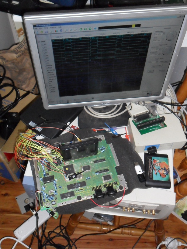
One of the big things about the VDP that's currently unknown is exactly when various bits of data are latched from VRAM during a scanline, and when external reads and writes are allowed into VRAM relative to them. This information is essential in order to be able to accurately respond to mid-line changes to the contents of VRAM. Unfortunately, the only real way to know this for sure is to use a logic analyzer to snoop on the activity over the private VRAM bus during operation, which needs specialized equipment and a modified Mega Drive in order to do. Erm, like this:
I could post a lot of information about exactly how the VDP uses the VRAM, how the memory is addressed, the bus logic used to handle data transfer, etc, but I don't want to take too long right now writing up pages and pages of information which isn't really directly helpful for emulation. I'll post all this stuff later when I formally write up all my notes on the VDP as a whole.
Here's what you need to know in order to understand the timing diagrams:
1. The VDP has a Serial Clock (SC) which drives access to VRAM. SC is twice the "pixel clock", IE, there are two SC ticks for every pixel output by the VDP. When running in H40 mode, SC is equivalent to EDCLK. When running in H32 mode, SC is equivalent to MCLK/5.
2. Every VRAM bus operation effectively takes 4 SC cycles. It's a bit more complicated than that in reality (operations actually take 7 SC cycles, but 3 cycles of each operation overlap), but when thinking about VRAM access, you can simply consider each access to VRAM takes 4 SC cycles, or in other words, two pixels are output by the VDP for every one access to VRAM.
3. Within each 4 SC read cycle, 4 bytes are read (4 nybbles from each VRAM chip in parallel).
4. Within each 4 SC write cycle, 1 byte is written (1 nybble to each vRAM chip in parallel)
5. A refresh cycle takes 4 SC cycles, within which nothing can be read or written.
So, now that you know all that, here are my timing notes (I hope you can understand my writing):
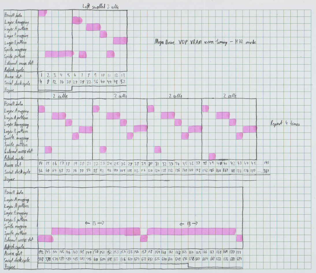
Here's some additional things you need to know about these notes:
1. For layers A and B, two mapping pairs (IE, 4 bytes) are read in each mapping read slot.
2. A single row of pixels (4 bytes) is read for each pattern read slot. Only the row of pixels within a cell which is visible on the current scanline is read, so when a block mapping references a cell, only 4 bytes are read, returning an 8 pixel row from that cell.
3. Sprite mapping data is read in the order sprites are parsed according to the link data. If there are no more sprites on the current scanline, any remaining sprite mapping read slots are wasted. They don't become available for external VRAM access.
4. Sprite pattern data is read in the order the mapping data is read, with the order being left to right for cells within a single sprite. If there are no more sprites on the current scanline, any remaining sprite pattern read slots are wasted. They don't become available for external VRAM access.
5. As you can see, sprite pattern data is finished being read at the start of the scanline, and then is used to display pixels on that scanline. This means for each scanline, all the mapping data for every sprite, and most of the pattern data, is read during the previous line.
6. The first read of layer A and B pattern data at the start of the line is used to read in an additional 2 cell block for each layer, to support horizontal scrolling (IE, even though the display may be, for example, 32 cells wide, 33 cells might be visible due to scrolling). If the cells in layer A and B are perfectly aligned to the screen, so that every cell is entirely visible, these additional reads are still performed, but the results are not used.
7. Only the last 4 bytes of each 8-byte sprite attribute entry are read from VRAM, containing the block mapping for the sprite, and the horizontal position. The first 4 bytes, containing the vertical position, size, and link data, are cached internally in the VDP, as per the notes already published here about sprite attribute table caching.
I hope you guys find this info useful. Feel free to ask any questions.
One of the big things about the VDP that's currently unknown is exactly when various bits of data are latched from VRAM during a scanline, and when external reads and writes are allowed into VRAM relative to them. This information is essential in order to be able to accurately respond to mid-line changes to the contents of VRAM. Unfortunately, the only real way to know this for sure is to use a logic analyzer to snoop on the activity over the private VRAM bus during operation, which needs specialized equipment and a modified Mega Drive in order to do. Erm, like this:
I could post a lot of information about exactly how the VDP uses the VRAM, how the memory is addressed, the bus logic used to handle data transfer, etc, but I don't want to take too long right now writing up pages and pages of information which isn't really directly helpful for emulation. I'll post all this stuff later when I formally write up all my notes on the VDP as a whole.
Here's what you need to know in order to understand the timing diagrams:
1. The VDP has a Serial Clock (SC) which drives access to VRAM. SC is twice the "pixel clock", IE, there are two SC ticks for every pixel output by the VDP. When running in H40 mode, SC is equivalent to EDCLK. When running in H32 mode, SC is equivalent to MCLK/5.
2. Every VRAM bus operation effectively takes 4 SC cycles. It's a bit more complicated than that in reality (operations actually take 7 SC cycles, but 3 cycles of each operation overlap), but when thinking about VRAM access, you can simply consider each access to VRAM takes 4 SC cycles, or in other words, two pixels are output by the VDP for every one access to VRAM.
3. Within each 4 SC read cycle, 4 bytes are read (4 nybbles from each VRAM chip in parallel).
4. Within each 4 SC write cycle, 1 byte is written (1 nybble to each vRAM chip in parallel)
5. A refresh cycle takes 4 SC cycles, within which nothing can be read or written.
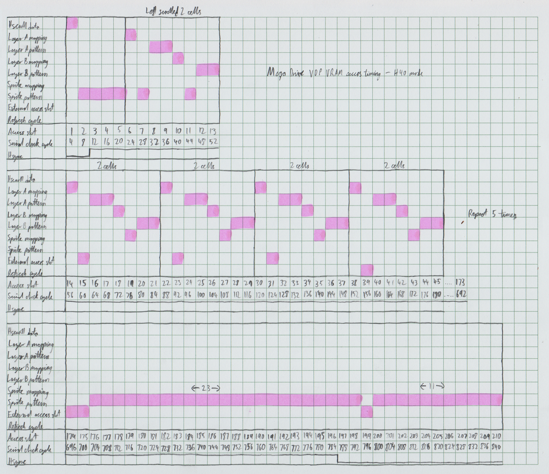
So, now that you know all that, here are my timing notes (I hope you can understand my writing):
Here's some additional things you need to know about these notes:
1. For layers A and B, two mapping pairs (IE, 4 bytes) are read in each mapping read slot.
2. A single row of pixels (4 bytes) is read for each pattern read slot. Only the row of pixels within a cell which is visible on the current scanline is read, so when a block mapping references a cell, only 4 bytes are read, returning an 8 pixel row from that cell.
3. Sprite mapping data is read in the order sprites are parsed according to the link data. If there are no more sprites on the current scanline, any remaining sprite mapping read slots are wasted. They don't become available for external VRAM access.
4. Sprite pattern data is read in the order the mapping data is read, with the order being left to right for cells within a single sprite. If there are no more sprites on the current scanline, any remaining sprite pattern read slots are wasted. They don't become available for external VRAM access.
5. As you can see, sprite pattern data is finished being read at the start of the scanline, and then is used to display pixels on that scanline. This means for each scanline, all the mapping data for every sprite, and most of the pattern data, is read during the previous line.
6. The first read of layer A and B pattern data at the start of the line is used to read in an additional 2 cell block for each layer, to support horizontal scrolling (IE, even though the display may be, for example, 32 cells wide, 33 cells might be visible due to scrolling). If the cells in layer A and B are perfectly aligned to the screen, so that every cell is entirely visible, these additional reads are still performed, but the results are not used.
7. Only the last 4 bytes of each 8-byte sprite attribute entry are read from VRAM, containing the block mapping for the sprite, and the horizontal position. The first 4 bytes, containing the vertical position, size, and link data, are cached internally in the VDP, as per the notes already published here about sprite attribute table caching.
I hope you guys find this info useful. Feel free to ask any questions.

