Thanks a lot for this, I'm impatiently waiting for your documentation.Actually, the dots that appear are the colour of the value you write. Essentially, when you write to CRAM, the single pixel that is being drawn at that moment displays the colour you were writing to the CRAM at that moment, regardless of the colour that should have been displayed. This occurs even when the display is disabled, or when the VDP is rendering the screen boarders, and one write always changes the colour of a single pixel if the VDP is in the process of rasterizing a line.
I've done extensive testing on this behaviour. You can actually use it to measure the timing of the FIFO buffer during active scan, as it allows you to see visually on the screen when each CRAM write gets through. I've emulated mid-line writes to CRAM, as well as this flicker bug, in my emulator. As for other settings though, like when specific register changes take effect, I haven't sampled that information yet. I'm planning to test each and every register setting, and writes to all the various buffers in ram to determine when the VDP samples all its data, and compile the results into a single document. It's essential in order to get the VDP emulation "perfect", and avoid all potential single-line raster problems like the one in Galahad, so I'll definitely be doing it at some point.
I may as well add a bit more info, I've noticed from observing the FIFO timing that there are a series of "slots" in fixed positions for each scanline when buffered writes go through. I'll be calculating the precise coordinates for those quite soon, but they appear to be 2 cells apart starting from the left side of the screen. There was also one mark in an odd position near the end of each line, which I believe corresponds with the position where the HINT is triggered.
There are a number of factors that lead me to believe that the VDP renders the screen in 2-cell segments internally, and it is logical that the only time data can be changed and produce predictable results is at the end of each of these 2 cell blocks, which the FIFO enforces. I suspect changes to ram are seen at the end of each of these blocks, but there are some questionable values, like hscroll data which I'd have to test to be sure, and I very much doubt mid-line changes to the sprite table are seen. As for register changes, I suspect these are only applied at some point during hblank. Again, this needs testing though.
Currently, I think I have finally achieved a 100% accurate VDP emulation since I can not find anymore games with single line glitches or flickering (but who know, testing ALL genesis games take sooo much time
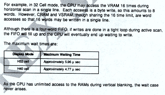
About the FIFO, the documentation give the max number of permitted CPU access to V-RAM by line (btw, data rate is likely the dma rate) , as well as the max waiting time for the FIFO to execute one command, did you figured the exact slot timesharing between VDP & CPU ? Can we consider taht a VRAM write and a VRAM read takes approximately the same number of VDP clock ?
About the sprites, you probably already know but Charles McDonald discovered that there was an internal copy of the SAT, when rendering sprites, some of the sprite attributes were taken from this table, some other taken from current VRAM table location
Most probably, sprite data is latched somewhere on the line.

