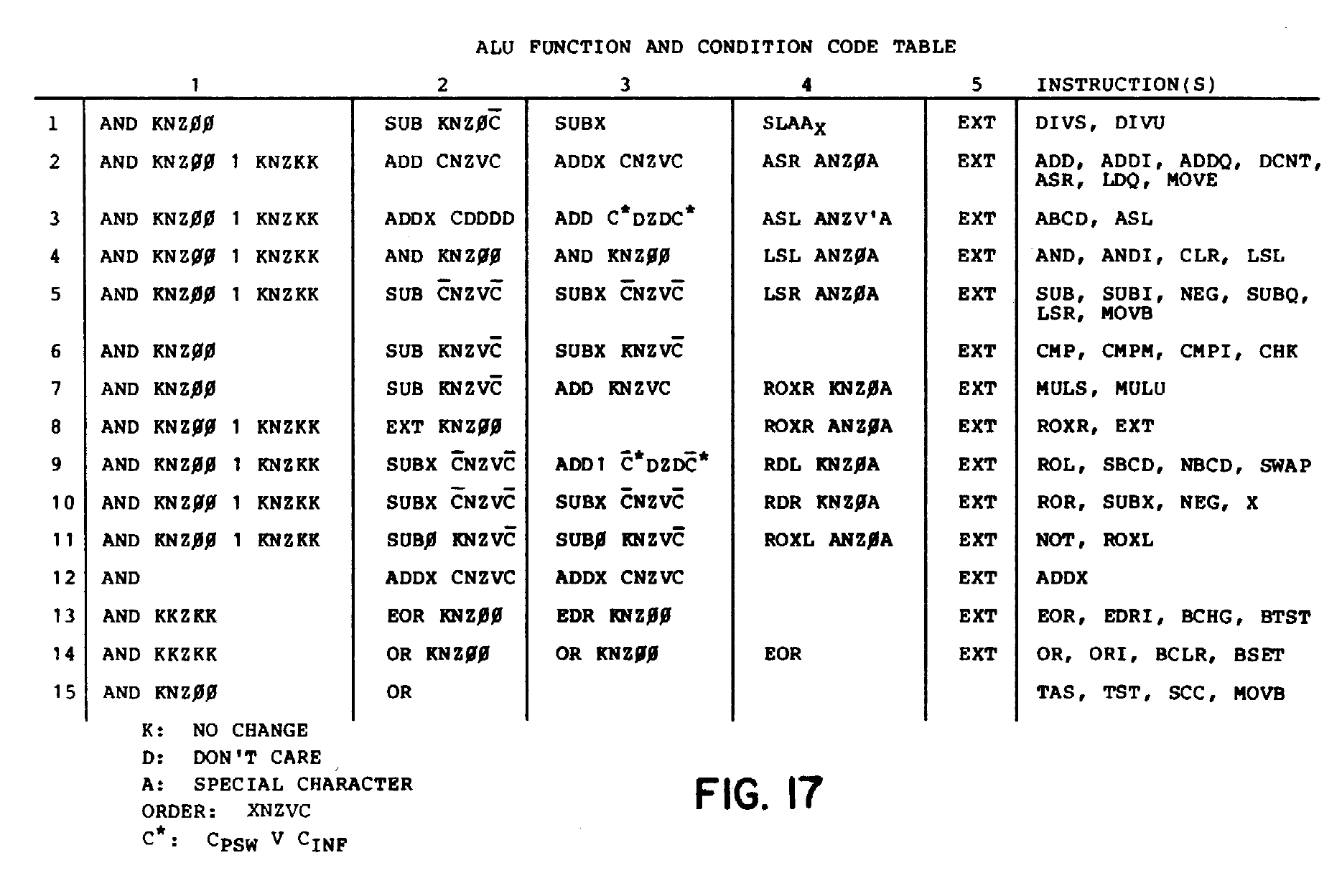
The Execution Unit
So far we've covered how to determine the sequence of microinstructions that are executed for a given macroinstruction (opcode). Now we'll dive into what those individual microinstructions can do. The most critical component for this is the Execution Unit. There's an entire separate patent on this that describes the execution unit in some detail, it's US4296469. (
https://nemesis.exodusemulator.com/M680 ... 296469.pdf). Here's figure 2 from that patent, which is also included in US4325121:
And here's a stitched together version of figure 3 which shows some more detail:
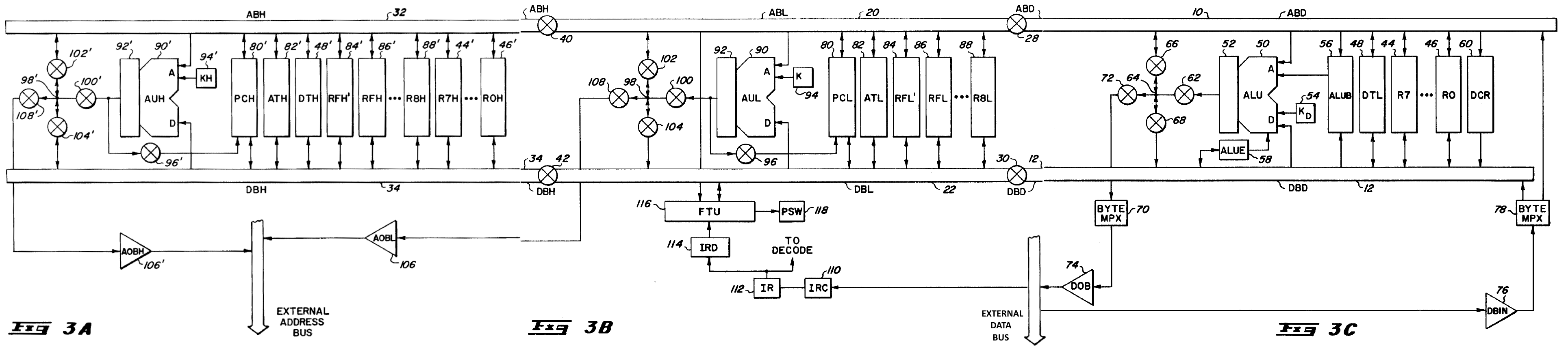
As we can see, the execution unit is broken into three separate parts, which are called from left to right "High Section", "Low Section", and "Data Section" respectively. The actual physical latches/flip-flops which store the register data are embedded within these sections, which combined together make up the "register file". Within each of the three sections of the execution unit there are separate arithmetic units, called AUH (Arithmetic Unit High), AUL (Arithmetic Unit Low), and ALU (Arithmetic Logic Unit) respectively. These units are capable of operating in parallel, and each have different capabilities. Finally, there are two main buses which connect everything together, called "Address Bus" and "Data Bus" respectively. These buses can be linked together or broken into three parts each at the boundaries between the sections. Almost all registers are dual-ported, meaning they can be connected to either the data bus or the address bus in their sections. This arrangement gives up to a total of 6 independent buses - Address bus high/low/data, and data bus high/low/data, and theoretically transfers can be occurring between registers/units on all 6 buses simultaneously.
Within the register file, there are a total of 21 32-bit registers. The arithmetic units are only 16-bits wide however, and all 32-bit registers are broken into 16-bit components and distributed between the sections. The high 16-bit parts of all 32-bit registers are contained within the "High" section. The low 16-bit components of "address" registers are contained in the "Low" section, while the low 16-bit components of "data" registers are contained in the "Data" section. Here's a key for the abbreviations given in the patent images above:
Code: Select all
AOB(H/L) - Address Output Buffer, a 32-bit latched register which stores the address value to output over the external address bus. Shown outside the execution unit as AOBH/AOBL above, but actually physically embedded within it like other registers. ["Memory address register" in Gigasoft analysis]
AT(H/L) = Address Temporary register ["immediate register" in Gigasoft analysis]
DT(H/L) = Data Temporary register ["Register B" in Gigasoft analysis]
PC(H/L) = Program Counter register
RF(H/L)' = SSP
RF(H/L) = USP
RE(H/L) = A6
RD(H/L) = A5
RC(H/L) = A4
RB(H/L) = A3
RA(H/L) = A2
R9(H/L) = A1
R8(H/L) = A0
R7(H/blank) = D7
R6(H/blank) = D6
R5(H/blank) = D5
R4(H/blank) = D4
R3(H/blank) = D3
R2(H/blank) = D2
R1(H/blank) = D1
R0(H/blank) = D0
where (H = Upper 16 bits (high), L or blank = Lower 16 bits (low))
This gives us a total of 21 32-bit registers in the main "register file". In addition, there are 10 16-bit registers within the register file:
Code: Select all
AUH Output - A latched (registered) 16-bit output from AUH (read-only, only AUH can modify) ["Register A" high 16 bits in Gigasoft analysis]
AUL Output - A latched (registered) 16-bit output from AUL (read-only, only AUL can modify) ["Register A" low 16 bits in Gigasoft analysis]
ALU Output - A latched (registered) 16-bit output from ALU (read-only, only ALU can modify) ["Register C" in Gigasoft analysis]
ALUB - ALU Buffer register - A 16-bit input register to ALU (write-only, only ALU can read) ["Register E" in Gigasoft analysis]
ALUE - ALU Extension register - A 16-bit register that can be generally read and written, but also acts as a special shift register for the ALU. ["Register G" in Gigasoft analysis]
DCR - DeCodeR, A latched 4-bit to 16-bit decoder register, takes a 4-bit input and outputs "1" on exactly one of the 16-bit data lines according to the value (IE, 0000 -> 0000000000000001, 0001 -> 0000000000000010, 0010 -> 0000000000000011, etc) ["Bit selection register (BIT#)" for input, "Selected bit (BIT)" for output on Gigasoft analysis]
DOB - Data Output Buffer, a 16-bit latched register which stores the value to output over the external data bus. ["Output Register" in Gigasoft analysis]
DBIN - Data Bus Input Buffer, a 16-bit latched register which stores the last data value read from the external data bus. ["Register D" in Gigasoft analysis]
FTU - Field Translation Unit, a 16-bit latched register which serves as an I/O buffer for reading/writing content stored in other regions of the processor, such as the status register, writing a trap vector to trigger an exception (eg, divide by zero), or extracting bits from the IRD register.
PREN - PRiority ENcoder, a 16-bit register which takes a MOVEM register bitmask as an input, and outputs a 4-bit register number representing the internal register number of the next register with a bit set. [[MOVEM register list (List) / next bit in register list in Gigasoft analysis]
In addition to these, there are the following registers physically and logically outside the register file, which also store data:
Code: Select all
IRC/IR/IRD - As described in the last post, these 16-bit registers make up the instruction prefetch and decode pipeline. IRC and IR are physically attached to the bottom of the execution unit, but aren't really within it. IRD is located elsewhere.
SR - Status Register, as described in the 68000 User's Manual. Contains condition code flags, interrupt mask, supervisor state, and trace mode flags. This isn't a complete 16-bit register, it's stored as a series of latched bits in different regions of the processor.
INL - 3-bit pending interrupt level
TPEND - Bit flag indicating trace pending when the current macroinstruction completes
So the execution unit contains a number of physical register storage buffers, some arithmetic units (AUH, AUL, ALU), and some special purpose units (FTU, DCR, PREN). Additionally, there is a small table of short constant values (IE, 0, +1, -2, +8, etc) which can be transferred directly into the various arithmetic units as inputs. The only thing the execution unit itself does is perform transfers to and from these various units/registers. With this understanding of the basic contents of the execution unit, we can now move onto looking at nanocode.
Nanocode
Nanocode is really like a big set of control lines telling the processor (and the execution unit in particular), what to do during a given microinstruction. When we're at this level, it's important to make a distinction between the "logical" view of the processor, IE, some abstract concept that can take a series of instructions and perform them, and the "physical" view of the processor, meaning an actual concrete machine made out of transistors. It is important to understand that the microcode formats in the patents describe processing steps for a "logical" processor, IE, they're the kind of thing they could write before they'd even built the physical circuits, they're the "spec" the circuits have to meet. As a result, some things are not specified, such as the exact order/timing things occur in, or in some cases even what buses are used to perform transfers within the execution unit.
More on that in a little bit. For now, let's have a look at some nanocode. We're going to look at "NOP" again:
Code: Select all
 ____________________________________
|                      <    |        |
| au --> db --> aob,au,pc   | irix   | mmrw3
| +2 --> au                 |--------|
|                           | dbi    |
|                           |--------|
|                           | x      |
|                           |--------|
|                           | dxdy   |
|___________________________|________|
|      213  |   b        |   b       |
\------------------------------------/

 ____________________________________
|                      >    |        |
| edb --> dbin,irc          | frix   |
| (ir) --> ird              |--------|
|                           | a1     |
|                           |--------|
|                           | x      |
|                           |--------|
|                           |        |
|___________________________|________|
|       26  |   mmrw3    |   mmrw3   |
\------------------------------------/
Each of these microinstructions have some nanocode shown. The nanocode uses many abbreviations. To understand what they mean, we turn to "Appendix B" in the patent, which transcribed is this:
Code: Select all
abbreviation     | meaning
------------------------------------------------------------------------------------------
rx               | register (data or address) designated by Rx field in macroinstruction
  rxa            | address register designated by Rx field in macroinstruciton
  rxd            | data register designated by Rx field in macroinstruction
  rxh            | upper half (16 most significant bits) of register (data or address) designated by Rx field in macroinstruction
  rxl            | lower half (16 least significant bits) of register (data or address) designated by Rx field in macroinstruction
  rxdl           | lower half (16 least significant bits) of data register designated by Rx field in macroinstruction
ry               | register (data or address) designated by Ry field in macroinstruction
  rya            | address register designated by Ry field in macroinstruciton
  ryd            | data register designated by Ry field in macroinstruction
  ryh            | upper half (16 most significant bits) of register (data or address) designated by Ry field in macroinstruction
  ryl            | lower half (16 least significant bits) of register (data or address) designated by Ry field in macroinstruction
  rydl           | lower half (16 least significant bits) of data register designated by Ry field in macroinstruction
rz               | register (data or address) designated by 4-bit field of second word of macro-instructions using indexed addressing for specifying register to be used as the index
  rzl            | lower half (16 least significant bits) of register described immediately above
db               | DATA BUS (including high, low and data sections)
  dbh            | DATA BUS (high section only)
  dbl            | DATA BUS (low section only)
  dbd            | DATA BUS (data section only)
  db*            | DATA BUS (at least data section)
dbe              | sign extend sign bit onto high section of DATA BUS
edb              | external data bus
dbin             | data bus input buffer (including a latch) coupled to external data bus
  dbinh          | upper byte (8 most significant bits) of data bus input buffer
  dbinl          | lower byte (8 least significant bits) of data bus input buffer
dob              | data bus output buffer coupled to external data bus
  dobh           | upper byte (8 most significant bits) of data bus output buffer
  dobl           | lower byte (8 least significant bits) of data bus output buffer
ab               | ADDRESS BUS (including high, low and data sections)
  abh            | ADDRESS BUS (high section only)
  abl            | ADDRESS BUS (low section only)
  abd            | ADDRESS BUS (data section only)
  ab*            | ADDRESS BUS (at least data section)
abe              | sign extend sign bit onto high section of ADDRESS BUS
aob              | address bus output buffer coupled to external address bus
*                | ADDRESS BUS (high, low and data sections) or alternatively DATA BUS (high, low and data sections)
*e               | sign extend sign bit onto high section of ADDRESS BUS or alternatively onto high section of DATA BUS
psw              | program status word which stores condition codes, interrupt level, trace mode bit, supervisor mode bit
psws             | supervisor mode bit in the program status word
ssw              | special word which monitors status of current microinstruction; accessed in event of address error or bus error to aid processor in recovery from error
at               | temporary address register
  ath            | upper half (16 most significant bits) of temporary address register
  atl            | lower half (16 least significant bits) of temporary address register
sp               | user or supervisor stack pointer
  sph            | upper half (16 most significant bits) of user or supervisor stack pointer
  spl            | lower half (16 least significant bits) of user or supervisor stack pointer
pc               | program counter register
  pch            | upper half (16 most significant bits) of program counter register
  pcl            | lower half (16 least significant bits) of program counter register
dcr              | decoder in data section of execution unit which is used for bit manipulation
'reset pren'     | used during instruction which specifies access to multiple registers in order to advance encoder to the address of the next register to be accessed
ftu              | field translation unit
'idle wait'      | no transfers occur during this microcycle
tpend            | a one-bit latch which indicates whether the current macroinstruction should implement a trace upon completion ot the macroinstruction
inl              | latch which stores the interrupt level of the interrupting device upon recognition of an interrupt for subsequent transfer into program status word
trap             | stores vector which can be supplied to field translate unit for addressing a trap routine in event of trap condition (e.g. divide-dy-zero)
corf             | correction factor for decimal arithmetic which can be provided to ALU
'sr c-alu-alue'  | shift right used in multiply operation; carry bit coupled to msb of ALU; lsb of ALU coupled to msb of ALUE
This list is incomplete however. To it, I'm going to add a set of additional entries and list their meanings, all of which have already been introduced/discussed above:
Code: Select all
abbreviation     | meaning
------------------------------------------------------------------------------------------
au               | AUH (Arithmetic Unit High) and AUL (Arithmetic Unit Low) working together on a 32-bit value
alu              | ALU (Arithmetic Logic Unit) working on a 16-bit value
irc              | Instruction Register Capture register, top of prefetch pipeline.
ir               | Instruction Register, next macroinstruction to execute.
ird              | Instruction Register Delay register, current macroinstruction being executed.
alub             | ALU Buffer register
alue             | ALU Extension register
Now that we have our handy list of what each of these abbreviations mean, we'll now look at the format entries in the nanocode listing take. The nanocode is listed as a series of sequential lines. From our "b" microinstruction, the A1 address for NOP, the nanocode is as follows:
What this nanocode is doing is listing two separate data transfer operations that are performed by the execution unit during the two clock cycles this microinstruction runs for. All nanocode will be a list like this, with each line in one of the three following forms:
Code: Select all
<source> --> <targetList>:  Transfer data from <source> into <targetList>
<source> --> <bus> --> <targetList>: Transfer data from <source> into <targetList> via <bus>
<keyword>: Special keyword such as 'reset pren' or 'idle wait', defined above.
where <targetList> is a comma separated list of one or more targets, such as "aob,au,sp".
Note that as shown here, a single source can potentially be written to multiple registers/units in one step. These aren't separate operations, when data is being moved over a bus, that's a set of physical lines which have the source value loaded. If more than one target is set to be updated, they will all receive the same value at the same time. What about subsequent lines however? When we have two transfer operations as shown above, what order are they performed in? That comes down to a question of the "logical" vs the "physical" processor I mentioned before. The nanocode is describing a "logical", or "theoretical" processor. From that perspective, the list of nanocode instructions are "sequentially consistent", or in other words, if you ran the operations one at a time in the order listed, that sequence describes the expected outcome when the same buses or registers are used more than once. The "physical" processor won't do them one at a time of course. As discussed, the execution unit can potentially perform six separate transfers "at once", but at the level we're now at, the implementation gets "creative" with timing in order to do as much in parallel as possible and squeeze everything into two clock cycles. Internally, there's all kinds of special "timing hacks" that are performed to sequence things "just right" so that it all works out in the right order, as described by the nanocode. The patents go into more detail in some areas, but suffice to say unless you're trying to fully replicate/understand the processor at the transistor level, it simply doesn't matter at this point. For my purposes, it suffices me to say that timing signals regulate the sequence of operations such that the execution unit produces a result consistent with the nanocode instructions being sequentially executed, but it does so within the microinstruction timing previously described (2 external clock cycles per microinstruction, unless an external bus transfer is being completed).
With this understanding of names, syntax and sequence, I'll now quickly reiterate the "preconditions" I listed in my last post that are assumed before each macroinstruction starts executing:
- IR and IRD both contain the first 16-bit instruction word (macroinstruction word) of the opcode about to be executed (IE, 0x4E71 for NOP)
- IRC contains the 16-bit value that immediately followed that 16-bit instruction word in memory (IE, possibly an extension word or a following macroinstruction word)
- PC contains the address the 16-bit value in IRC was fetched from (address of opcode about to be executed + 2)
- The "au" unit contains the address stored in PC + 2. (address of opcode about to be executed + 4)
With all this, we should now be able to understand the nanocode in these NOP microinstructions. Let's start with "b"
Code: Select all
// Transfer the 32-bit AUH/AUL contents to aob (address bus output buffer) and pc (program counter) via db (data bus high/low/data)
// Additionally, feed the same value back into AUH/AUL as one input.
au --> db --> aob,au,pc

// Feed the constant +2 into AUH/AUL as another input
+2 --> au
So this microinstruction has advanced PC by 2, put that address on the external data bus, and fed it back into the AU to have 2 added to it again. Note that the actual addition operation doesn't occur as part of this code, all we did was retrieve the output in the AU unit (AUH/AUL) from a previous operation, and provide inputs for a following operation. We'll look at how these operations are controlled soon as part of the "ALU function" section. For now suffice to say it'll happen. Let's look at the read operation for prefetch now though. If we go back to the microword definition, the "access label" for the "b" microinstruction was irix. Our "key" chart tells us that means that instruction
initiated a
read operation for an
immediate instruction parameter or a new instruction(
x). This will cause the processor to start a bus read operation at the address we placed in aob, with the "Function Code" lines set appropriately ("program" read in this case, not "data"). This microinstriction also had "next micro rom address" set to "dbi", which means after this instruction completes, IRC will be advanced to IR, so the A1/A2/A3 pointers will now reference the following opcode.
Now let's look at the following "mmrw3" microinstruction:
Code: Select all
// Transfer the contents of edb (external data bus) into dbin (data bus input buffer) and irc (instruction register capture).
// This is pulling in our prefetched 16-bit value which follows the next instruction after this one. It may or may not be a macroinstruction.
edb --> dbin,irc

// Load the next instruction being decoded into IRD to make it the "current" instruction
(ir) --> ird
After this instruction completes, its "next micro rom address" field is set to a1, so it will branch to the entry point for the next instruction we just moved into the IRD register. So all in all, what we've done is move IRC into IR, prefetch another word into IRC, and move IR into IRD and jump to the start of the next macroinstruction, which is exactly what we expect NOP to do. We've also updated "au" to maintain the correct preconditions for the next macroinstruction.
Microinstructions and bus timing
The NOP instruction we've been examining takes 4 clock cycles to perform, if there are no delays performing the read. A single bus read operation also takes 4 clock cycles if there are no delays. Let's look at how the NOP macroinstruction maps to bus operations. Here's a modified image ripped from the 68000 User's Manual:
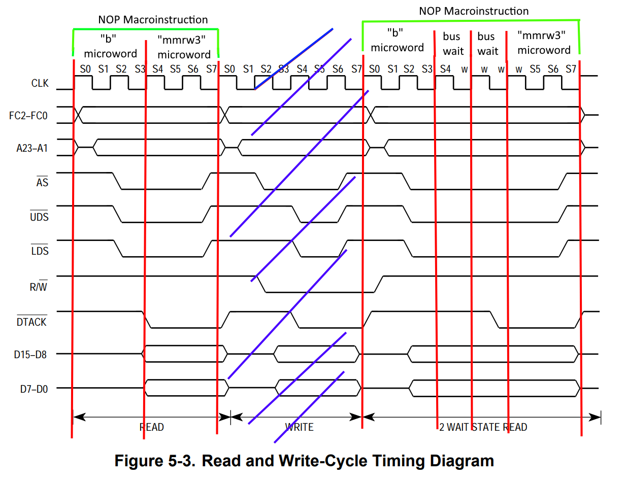
Here we see an example of a NOP instruction executing, a crossed out section where "something else" happens in the middle, then an example of a NOP instruction executing where there's a delay in the read occurring, due to external device latency responding to the read request. As you can see, the bus operation starts immediately as the "b" microinstruction begins executing. This can occur, because the microinstruction itself tells the processor that it will perform a read, and the kind of read (program/data) being performed, which is sufficient to begin signaling the read operation with the correct function code. You see this happening on the diagram above within the "S0" (State 0) period. Within "S1", the address lines are asserted. This is because the nanocode has been able to perform the "au --> db --> aob,au,pc" transfer by this point. "S2" then begins, and the processor drives the Address Strobe (AS) to signal the read request to external devices. Nothing changes during "S3", and now we've reached the end of the "b" microinstruction. Here's the important point - the CPU is now waiting for the read to complete, and we're "between microinstructions". At this point, the processor waits for the bus operation to complete, IE, by DTACK or BERR being asserted. Until that occurs, the processor inserts full clock cycles, and just sits there, waiting, not beginning the new microinstruction. If DTACK is signaled at that magic edge of the clock cycle, the data is latched, and the "mmrw3" microinstruction will immediately begin. If BERR is signaled at the edge of the clock cycle, the group 0 bus error exception will be made pending, and rather than executing "mmrw3", the A0S microcode address will overwrite the target address and the bus error exception handler will trigger instead.
An address exception is similar. The "b" microinstruction executes as normal, however if an unaligned read is attempted triggering an address error, at the start of "S2" rather than asserting AS, the processor will flag a pending address error and set the A0S microcode address to the address errror exception handler, which will execute next rather than "mmrw3". Note that the external function code and address lines will still be asserted prior to the address exception being detected, but since AS isn't asserted this will be ignored by external devices.
That'll do for now. I'll write more about the ALU and more complex instructions later.
EDIT: Added info on address exceptions.