M68000 Microcode-level emulation
Posted: Mon Mar 19, 2012 2:29 am
I've become very interested as of late in taking M68000 emulation to a new level. I have written an extremely accurate M68000 core for my emulator. From what I've seen, it's more accurate than the one in MAME. That said, it still has some fundamental limits on its accuracy, which I've become increasingly aware are virtually unsolveable with the way my core is designed.
Here's the issue: The M68000 is microcoded, meaning every single machine code instruction the CPU reads isn't really an instruction for the CPU directly, it's more like a key, telling it what set of internal instructions to execute. In a way, microcode is kind of like a data table the CPU uses internally to map these high-level "macro" instructions down to a set of real-low level internal operations to execute. A single opcode for example may actually be made up of a dozen internal operations, or internal execution steps. Effectively, a micro-coded processor is a little like a RISC machine with a very basic, small instruction set, emulating a CISC machine with a more complex and larger instruction set, but in this case, the emulation layer is built into the processor.
Now all of this may seem irrelivent for emulation purposes. This is internal detail afterall, and how something is actually implemented internally doesn't really matter from an emulation point of view, as long as it appears to behave identically from an external point of view. The problem is, there are a lot of quirks with M68000 instructions that occur due to the way things are done on the microcode level, which are visible from outside the M68000, in the way it performs external bus operations. Sometimes, this sub-opcode timing and behaviour is critical. The most obvious example on the Mega Drive relates to bus requests. It's possible to perform a long-word write to the VDP for example, where the first half of the write triggers a DMA transfer operation, and the second word, for example, modifies a VDP register. In this case, on the real hardware, the first write would be performed, which would trigger the VDP to request the bus, which would cause the M68000 to yeild the bus before the second word write was performed. The VDP would then perform the DMA transfer, release the bus, and be ready to receive command port data again by the time the second half of the long-word write sends data to the VDP command port again. There are games that rely on this behaviour I believe. Things get more critical where you add on systems like the MegaCD and 32x, where you have half a dozen processors sharing buses. Suddenly you can have timing problems if one processor doesn't yeild the bus to another in a timely manner.
There are other cases where microcode level emulation can be important. In particular, if you emulate at the opcode level, there's no indication on the exact order of reads and writes to the external bus, especially if you also care about the order of reads and writes for an opcode relative to the instruction pre-cache operations. Some opcodes have surprising orders of reads and writes when breaking up long-word bus operations into word operations, one of which is described in this document:
http://web.archive.org/web/200910151327 ... knotes.txt
There's another good document giving a fairly comprehensive description of when pre-caching occurs for a large number of instructions:
http://pasti.fxatari.com/68kdocs/68kPrefetch.html
Both of these documents are very incomplete in their coverage though, and all of this is still ignoring timing issues, IE, if you want to actually get an M68000 core which performs not just the correct sequence, but the correct timing, between external bus operations, the information simply doesn't exist in the public domain. All of this can be critical when working with memory-mapped hardware, and the order of operations is critical with group 0 exception handling.
One of the biggest problems with an opcode-level M68000 is actually the code structure. You could try and retro-fit workarounds for some of this low-level order and timing behaviour into an opcode-level M68000 emulation core, but how do you make that core correctly respond to group 0 exceptions, and supports savestates, when you don't emulate at the microcode level? If you consider an opcode the smallest non-divisible unit of work in your M68000 core, exactly how do you write a generic core which can yeild the bus halfway through any long-word operation, or between every bus operation in that opcode? How do you generate a savestate when your M68000 core is in this state? What if you have memory-mapped hardware which is designed to request the bus after a read, and it's critical to have it obtain it before the next write to that address? How do you support that for every opcode which potentially performs a read followed by a write?
Now, some of these problems can be worked around on a specific case-by-case basis, depending on what's important for a given system. I'd like to write a "perfect" M68000 core that just does everything right for all instructions though, and it's becoming clear to me that the only practical way to make that happen is to gather much lower level information about how the M68000 uses the bus. I have a logic analyser, and I was planning on snooping on the M68000 bus to determine the correct bus access order and timing of every M68000 opcode. I'll probably still do this. I realised this wouldn't solve some of the more fundamental design problems I'm presented with though, like how to correctly support yielding the bus at all the correct points, during opcode execution. This has led me to look at another approach.
I've been very interested of late in the incredible work that's been done on the 6502 processor, where they've successfully decapped the chip, analysed and decyphered all the internal connections within the die, and emulated the entire chip on the transistor level (check it out here: http://www.visual6502.org ). This is a level of emulation which is totally insane, and I take my hat off to the guys who pulled this off. It's got me thinking though. We have complete, high resolution die shots of the entire M68000 die:
http://www.visual6502.org/images/pages/ ... 68000.html
Thanks to Motorola, we have a basic block diagram of what areas of the die perform what functions:
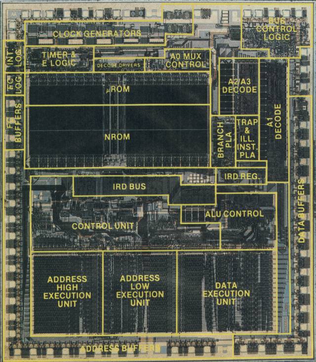
(sourced from http://www.easy68k.com/paulrsm/doc/dpbm68k2.htm , the original image comes from Motorola, I've seen it referenced in books such as "68000, 68010, 68020 Primer", page 42, which you can download from http://www.scribd.com/doc/29071553/6800 ... 020-Primer)
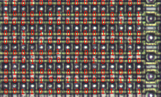
We can see from this image two clear banks of ROM data, one containing microcode (marked as µROM), and one containing nanocode (marked as NROM). The machine code maps to microcode, which in tern maps to nanocode, which is what triggers the actual internal operations performed by the M68000 CPU. For any Z80 gurus, this is "similar" to the M and T states in the Z80, where nanocode instructions are your T cycles, and microcode instructions are your M cycles. What I want to do is "decode" this internal ROM data, that is, figure out how it's used, and reverse-engineer a complete, accurate description of each stage of execution for each opcode. Effectively, I want to decode the internal microcode/nanocode instructions, so that we can emulate the M68000 on the microcode/nanocode level, rather than the opcode level like every M68000 core is currently doing. I've been analysing the die shots, and I'm making progress. Based on some careful observation and cross-referencing with other decapping projects where internal ROM data has been read, in particular the work done in decapping the YM3812 ( http://yehar.com/blog/?p=665 ), I'm now able to visually read the internal ROM data from the M68000 die shots:
Now I'm trying to take this to the next level, and start figuring out how an opcode maps to this ROM data, and how this ROM data drives the internal functions within the M68000. I'm actively researching this right now and making some progress.
Here's what's obvious/well known:
-The first 16-bit command word of each M68000 opcode is enough to define the instruction, and get loaded into an internal instruction register (IRD)
-The upper 4 bits of each opcode act as a main key, describing the high-level "category" of the opcode
-Opcodes take multiple cycles to execute
-Each nanocode "instruction" takes one cycle to execute
-An internal cycle counter of some kind must be kept to track the current progression through the execution of an opcode
It seems as though this ROM data probably acts as a table, with the combination of the instruction register and the cycle counter used as a key into the table. I'm guessing the upper 4 bits of the instruction register are used as a key into microcode ROM, which in tern gives some kind list of keys into the nanocode ROM. For each microcode instruction, multiple nanocode instructions may be run. The last nanocode instruction run for each opcode (except some special cases like the STOP opcode), is an instruction which resets the cycle counter and loads the instruction pre-cache (IR) into the instruction word (IRD). This means the next cycle will start executing that instruction.
What I want to do is open this research up to a larger audience than just, well, me. I'm interested in any feedback, comments, suggestions, and in particular, anyone who knows more about internal CPU architecture than me (which is to say, pretty much anything), who might be able to contribute with decyphering this thing. I'm trying to make sense of the M68000 die shot, but I have no previous experience with this. It's a bit like staring at a document you know holds the answers to all your questions, but it's written in ancient egyptian heiroglyphs, and you can only read yiddish.
Here's the issue: The M68000 is microcoded, meaning every single machine code instruction the CPU reads isn't really an instruction for the CPU directly, it's more like a key, telling it what set of internal instructions to execute. In a way, microcode is kind of like a data table the CPU uses internally to map these high-level "macro" instructions down to a set of real-low level internal operations to execute. A single opcode for example may actually be made up of a dozen internal operations, or internal execution steps. Effectively, a micro-coded processor is a little like a RISC machine with a very basic, small instruction set, emulating a CISC machine with a more complex and larger instruction set, but in this case, the emulation layer is built into the processor.
Now all of this may seem irrelivent for emulation purposes. This is internal detail afterall, and how something is actually implemented internally doesn't really matter from an emulation point of view, as long as it appears to behave identically from an external point of view. The problem is, there are a lot of quirks with M68000 instructions that occur due to the way things are done on the microcode level, which are visible from outside the M68000, in the way it performs external bus operations. Sometimes, this sub-opcode timing and behaviour is critical. The most obvious example on the Mega Drive relates to bus requests. It's possible to perform a long-word write to the VDP for example, where the first half of the write triggers a DMA transfer operation, and the second word, for example, modifies a VDP register. In this case, on the real hardware, the first write would be performed, which would trigger the VDP to request the bus, which would cause the M68000 to yeild the bus before the second word write was performed. The VDP would then perform the DMA transfer, release the bus, and be ready to receive command port data again by the time the second half of the long-word write sends data to the VDP command port again. There are games that rely on this behaviour I believe. Things get more critical where you add on systems like the MegaCD and 32x, where you have half a dozen processors sharing buses. Suddenly you can have timing problems if one processor doesn't yeild the bus to another in a timely manner.
There are other cases where microcode level emulation can be important. In particular, if you emulate at the opcode level, there's no indication on the exact order of reads and writes to the external bus, especially if you also care about the order of reads and writes for an opcode relative to the instruction pre-cache operations. Some opcodes have surprising orders of reads and writes when breaking up long-word bus operations into word operations, one of which is described in this document:
http://web.archive.org/web/200910151327 ... knotes.txt
There's another good document giving a fairly comprehensive description of when pre-caching occurs for a large number of instructions:
http://pasti.fxatari.com/68kdocs/68kPrefetch.html
Both of these documents are very incomplete in their coverage though, and all of this is still ignoring timing issues, IE, if you want to actually get an M68000 core which performs not just the correct sequence, but the correct timing, between external bus operations, the information simply doesn't exist in the public domain. All of this can be critical when working with memory-mapped hardware, and the order of operations is critical with group 0 exception handling.
One of the biggest problems with an opcode-level M68000 is actually the code structure. You could try and retro-fit workarounds for some of this low-level order and timing behaviour into an opcode-level M68000 emulation core, but how do you make that core correctly respond to group 0 exceptions, and supports savestates, when you don't emulate at the microcode level? If you consider an opcode the smallest non-divisible unit of work in your M68000 core, exactly how do you write a generic core which can yeild the bus halfway through any long-word operation, or between every bus operation in that opcode? How do you generate a savestate when your M68000 core is in this state? What if you have memory-mapped hardware which is designed to request the bus after a read, and it's critical to have it obtain it before the next write to that address? How do you support that for every opcode which potentially performs a read followed by a write?
Now, some of these problems can be worked around on a specific case-by-case basis, depending on what's important for a given system. I'd like to write a "perfect" M68000 core that just does everything right for all instructions though, and it's becoming clear to me that the only practical way to make that happen is to gather much lower level information about how the M68000 uses the bus. I have a logic analyser, and I was planning on snooping on the M68000 bus to determine the correct bus access order and timing of every M68000 opcode. I'll probably still do this. I realised this wouldn't solve some of the more fundamental design problems I'm presented with though, like how to correctly support yielding the bus at all the correct points, during opcode execution. This has led me to look at another approach.
I've been very interested of late in the incredible work that's been done on the 6502 processor, where they've successfully decapped the chip, analysed and decyphered all the internal connections within the die, and emulated the entire chip on the transistor level (check it out here: http://www.visual6502.org ). This is a level of emulation which is totally insane, and I take my hat off to the guys who pulled this off. It's got me thinking though. We have complete, high resolution die shots of the entire M68000 die:
http://www.visual6502.org/images/pages/ ... 68000.html
Thanks to Motorola, we have a basic block diagram of what areas of the die perform what functions:
(sourced from http://www.easy68k.com/paulrsm/doc/dpbm68k2.htm , the original image comes from Motorola, I've seen it referenced in books such as "68000, 68010, 68020 Primer", page 42, which you can download from http://www.scribd.com/doc/29071553/6800 ... 020-Primer)
We can see from this image two clear banks of ROM data, one containing microcode (marked as µROM), and one containing nanocode (marked as NROM). The machine code maps to microcode, which in tern maps to nanocode, which is what triggers the actual internal operations performed by the M68000 CPU. For any Z80 gurus, this is "similar" to the M and T states in the Z80, where nanocode instructions are your T cycles, and microcode instructions are your M cycles. What I want to do is "decode" this internal ROM data, that is, figure out how it's used, and reverse-engineer a complete, accurate description of each stage of execution for each opcode. Effectively, I want to decode the internal microcode/nanocode instructions, so that we can emulate the M68000 on the microcode/nanocode level, rather than the opcode level like every M68000 core is currently doing. I've been analysing the die shots, and I'm making progress. Based on some careful observation and cross-referencing with other decapping projects where internal ROM data has been read, in particular the work done in decapping the YM3812 ( http://yehar.com/blog/?p=665 ), I'm now able to visually read the internal ROM data from the M68000 die shots:
Now I'm trying to take this to the next level, and start figuring out how an opcode maps to this ROM data, and how this ROM data drives the internal functions within the M68000. I'm actively researching this right now and making some progress.
Here's what's obvious/well known:
-The first 16-bit command word of each M68000 opcode is enough to define the instruction, and get loaded into an internal instruction register (IRD)
-The upper 4 bits of each opcode act as a main key, describing the high-level "category" of the opcode
-Opcodes take multiple cycles to execute
-Each nanocode "instruction" takes one cycle to execute
-An internal cycle counter of some kind must be kept to track the current progression through the execution of an opcode
It seems as though this ROM data probably acts as a table, with the combination of the instruction register and the cycle counter used as a key into the table. I'm guessing the upper 4 bits of the instruction register are used as a key into microcode ROM, which in tern gives some kind list of keys into the nanocode ROM. For each microcode instruction, multiple nanocode instructions may be run. The last nanocode instruction run for each opcode (except some special cases like the STOP opcode), is an instruction which resets the cycle counter and loads the instruction pre-cache (IR) into the instruction word (IRD). This means the next cycle will start executing that instruction.
What I want to do is open this research up to a larger audience than just, well, me. I'm interested in any feedback, comments, suggestions, and in particular, anyone who knows more about internal CPU architecture than me (which is to say, pretty much anything), who might be able to contribute with decyphering this thing. I'm trying to make sense of the M68000 die shot, but I have no previous experience with this. It's a bit like staring at a document you know holds the answers to all your questions, but it's written in ancient egyptian heiroglyphs, and you can only read yiddish.