Hi guys. I've noticed there a number of people here with a lot more knowledge about the nitty gritty hardware of the humble Mega Drive than myself, so I thought I'd pose a few questions which I've been unable to figure out the answers to on my own.
I'm currently writing an emulator for the Mega Drive. This emulator, above all, is being built for accuracy, far beyond what is currently available. In some cases this requires information which is generally not required. In this case, I require some advanced info about the bus interactions within the Mega Drive.
I'm currently stuck. I have a strong background in programming, but my practical experience with digital electronics is somewhat lacking. I understand the external interfaces to the M68000 and Z80, and I understand completely how their bus cycles work, and how they interact with the external system. What I don't understand is how the bus circuitry of the external system itself is connected. Consider the following practical example. You have an M68000, with 10 separate memory mapped devices hanging off it. When the M68000 wants to read from a given memory address, in a nutshell, it sets R/W, places the address on the address lines, and asserts AS and LDS and or UDS as required, and waits for DTACK. The target external device senses that the strobes have been asserted, decodes the address, writes the data, and asserts DTACK. That's all well and good, and I get that. The critical part I don't understand is how a read from a particular address ends up being directed to one device, while a read from another address ends up at another device. What happens within the Mega Drive after those strobe lines are asserted so that the correct chip replies to the memory access? It's the physical bus connections between the M68000 and the external chipsets that I have been unable to decipher.
Now, this level of knowledge may seem unnecessary. Emulators usually just implement the flat memory map for a processor, look at the target address, and direct the memory access directly to the target chipset. That's what I'm doing currently, and it works, but I want to be able to model something which is a step further, and that's the ability to attach add-ons to a system.
If you look at the Pro Action Replay, it's able to intercept memory reads to the system RAM, and return a different value in its place. The PAR seems to be unable to intercept access to many other areas however, such as the VDP. I don't know if that's simply due to a limitation of the PAR itself, or if it's because it's impossible to intercept VDP access through the cartridge port. In the case of the Mega Drive, it's these rules I need to know. When reading and writing to memory addresses in the Mega Drive, what addresses are visible from the cartridge port, and what addresses are visible from the expansion port? I need to know what parts of the memory map an external device could potentially extend or override from these external connectors.
Obviously, the key to answering these questions is to understand how memory reads and writes are directed to different devices within the system. If you understand that system, the answers to those questions are immediately obvious, but I've been unable to figure it out so far, and it's beginning to hinder the development of my emulator.
I've got another original Model 1 Mega Drive on the way, and when it arrives I'll be desoldering everything off the board, scanning the board, and studying it. In the interim, I thought I may as well pose the question here. How do the links between devices in the Mega Drive work, such that memory access to a particular range goes to one chipset, while access to another range goes to another? Ultimately I would like to document and model this system of bus interactions within the Mega Drive, complete and in their entirety. Any information would be appreciated.
Workings of the Mega Drive: Bus Interactions
-
Mask of Destiny
- Very interested
- Posts: 628
- Joined: Thu Nov 30, 2006 6:30 am
Re: Workings of the Mega Drive: Bus Interactions
The Genesis/MD chipset decodes some of the 68K address lines to generate chip selects for RAM, the cartridge port, the side expansion port etc.Nemesis wrote:You have an M68000, with 10 separate memory mapped devices hanging off it. When the M68000 wants to read from a given memory address, in a nutshell, it sets R/W, places the address on the address lines, and asserts AS and LDS and or UDS as required, and waits for DTACK. The target external device senses that the strobes have been asserted, decodes the address, writes the data, and asserts DTACK. That's all well and good, and I get that. The critical part I don't understand is how a read from a particular address ends up being directed to one device, while a read from another address ends up at another device. What happens within the Mega Drive after those strobe lines are asserted so that the correct chip replies to the memory access? It's the physical bus connections between the M68000 and the external chipsets that I have been unable to decipher.
Peripherals on the cartridge and expansion ports can ignore these chip selects and do their own decoding, but that's not very common.
Technically the PAR shouldn't be able to intercept anything other than access to the cartridge. There's no mechanism to allow an external device to muck with the internal address mapping of the MD (well apart from the address swapping between the cartridge and expansion ports based on !CART_IN, but that's quite limited) and generally speaking have two different devices driving the bus at the same time is generally a bad idea. My best guess is that the PAR monitors the bus for writes to RAM and then somehow sneaks in another write before the 68K has a chance to read from it again, but I'm not exactly sure how it would pull that off either.If you look at the Pro Action Replay, it's able to intercept memory reads to the system RAM, and return a different value in its place. The PAR seems to be unable to intercept access to many other areas however, such as the VDP. I don't know if that's simply due to a limitation of the PAR itself, or if it's because it's impossible to intercept VDP access through the cartridge port.
There's two 4MB areas mapped to the external connectors. One at 0x0 and one at 0x400000. Which one is mapped where depends on the state of the !CART_IN line on the cartridge port. Additionally, two smaller areas in the A1XXXX range are mapped to separate chip selects on the cartridge port and expansion port (IIRC, A12XXX goes to the expansion port and A13XXX goes to the cartridge port).In the case of the Mega Drive, it's these rules I need to know. When reading and writing to memory addresses in the Mega Drive, what addresses are visible from the cartridge port, and what addresses are visible from the expansion port? I need to know what parts of the memory map an external device could potentially extend or override from these external connectors.
The 32X maps its hardware starting at 0x800000, but AFAIK it doesn't use any of the MD address decoding hardware to do it.
No need to trace a bunch of circuits. There's a complete MD1 schematic on Charles MacDonald's site ( http://cgfm2.emuviews.com/ ).I've got another original Model 1 Mega Drive on the way, and when it arrives I'll be desoldering everything off the board, scanning the board, and studying it. In the interim, I thought I may as well pose the question here. How do the links between devices in the Mega Drive work, such that memory access to a particular range goes to one chipset, while access to another range goes to another? Ultimately I would like to document and model this system of bus interactions within the Mega Drive, complete and in their entirety. Any information would be appreciated.
-
HardWareMan
- Very interested
- Posts: 753
- Joined: Sat Dec 15, 2007 7:49 am

Aha! That makes sense. So, the AS line from the M68000 would run into the "bus controller" or the like for the system (315-5364 for the original Model 1), and the controller outputs a whole set of lines such as ROM, CE0, ASEL, CAS0, RAS0, etc, which are set by the controller based on the target address (as per the diagram posted in http://www.spritesmind.net/_GenDev/foru ... .php?t=286 by HardWareMan), and these signals can then be used by external chips, perhaps directly as an AS line or through some other form of logic, to determine whether they will act on the bus request.The Genesis/MD chipset decodes some of the 68K address lines to generate chip selects for RAM, the cartridge port, the side expansion port etc.
Peripherals on the cartridge and expansion ports can ignore these chip selects and do their own decoding, but that's not very common.
Ok, so they're working some kind of voodoo to pull that off. I thought that what the PAR was actually doing was intercepting reads to the target address and returning another value in its place, but I've just done a few tests and confirmed the PAR definitely modifies the contents of the memory, so they probably just monitor memory access, then somehow steal or lock the bus for a brief period and sneak in their own writes. That makes things a lot simpler. No wonder I couldn't figure out how the PAR fitted in.Technically the PAR shouldn't be able to intercept anything other than access to the cartridge. There's no mechanism to allow an external device to muck with the internal address mapping of the MD (well apart from the address swapping between the cartridge and expansion ports based on !CART_IN, but that's quite limited) and generally speaking have two different devices driving the bus at the same time is generally a bad idea. My best guess is that the PAR monitors the bus for writes to RAM and then somehow sneaks in another write before the 68K has a chance to read from it again, but I'm not exactly sure how it would pull that off either.
Yeah, I knew about this behaviour, but I hadn't been able to figure out how it was achieved before. I'm guessing now that the bus controller changes its behaviour when CART is not asserted, so that whatever line acts as the main AS line for the expansion port triggers at 0x000000 instead of 0x400000, and likewise one or more of the lines running to the cartridge port change behaviour as well.There's two 4MB areas mapped to the external connectors. One at 0x0 and one at 0x400000. Which one is mapped where depends on the state of the !CART_IN line on the cartridge port.
Yep, TIME to the cartridge port at 0xA12XXX, and FDC to the expansion port at 0xA13XXX.Additionally, two smaller areas in the A1XXXX range are mapped to separate chip selects on the cartridge port and expansion port (IIRC, A12XXX goes to the expansion port and A13XXX goes to the cartridge port).
Yeah, I've got those schematics stitched together and printed out on nice big A3 pages with notes scribbled on them. Unfortunately, since all the bus lines run together into general address, data, and control rails, it's not always that easy to trace what's connected to a single line. Still, now that I've got a better idea of how the bus system works, the schematics make a lot more sense. I was beginning to think there was some kind of chained or priority-based system in use which was being hidden in the schematics by the combined groups.No need to trace a bunch of circuits. There's a complete MD1 schematic on Charles MacDonald's site
Thanks for your help MoD. I've been running around in circles with this one for a few weeks now.
A new question. There are a lot of lines in that vcontrol group. Does anyone have a document which describes them? I'm thinking that's something which would be an important companion to the schematic.
One "interesting" thing you can also see one the schematics is that the Bus Arbitrer takes only VD8 and ZD0 data lines... I presume it's because it only needs bit8 (bit 0 with 8bits access) of DATA bus when accessing the ZBUSREQ/ZBUSACK and ZRESET signals (bit8 in $A11100 and $A11200)
I also have a question about !TIME ($A130xx): when the software writes a 8bits value at these addresses, how is translated on the !TIME serial line ? Is there some kind of timing to send each bit ?
I also have a question about !TIME ($A130xx): when the software writes a 8bits value at these addresses, how is translated on the !TIME serial line ? Is there some kind of timing to send each bit ?
-
HardWareMan
- Very interested
- Posts: 753
- Joined: Sat Dec 15, 2007 7:49 am
I confirm that.Eke wrote:One "interesting" thing you can also see one the schematics is that the Bus Arbitrer takes only VD8 and ZD0 data lines... I presume it's because it only needs bit8 (bit 0 with 8bits access) of DATA bus when accessing the ZBUSREQ/ZBUSACK and ZRESET signals (bit8 in $A11100 and $A11200)
The !TIME signal acts like an ordinary CS signal. For data strobe you need to use CAS0/CAS2 for read and LWR/UWR for write. But when !TIME removed, data bus VD0-VD15 still have current data (when M68K do some write). That why you can simply connect !TIME to "clk" input of 7474 trigger (data latch on low-to-high). Understand why this is happening. All CS signals tied to signal AS, which shows that valid address on bus. Here is diagram from M68K Users Manual:Eke wrote:I also have a question about !TIME ($A130xx): when the software writes a 8bits value at these addresses, how is translated on the !TIME serial line ? Is there some kind of timing to send each bit ?

I see...
This mean that the value written at these adresses is then read from DATA bus by additional cart hardware (chip selected by !TIME), which also do some address decoding if multiple addresses can be used (for example, bankswitching at $A130Fx, see ssf2).
Is that correct ?
EDIT:ok,your edit answered my question, thanks
-
HardWareMan
- Very interested
- Posts: 753
- Joined: Sat Dec 15, 2007 7:49 am
I have an 10in1 cart, mapper on 161 register which latch data on VD0-VD3 on !TIME signal. Very simple bankswitching.Eke wrote:This mean that the value written at these adresses is then read from DATA bus by additional cart hardware (chip selected by !TIME), which also do some address decoding if multiple addresses can be used (for example, bankswitching at $A130Fx, see ssf2).
I've been studying the schematics in some detail, trying to figure out how each possible interaction between the chipsets happen, and I'm realising how complex the banked memory access to the M68000 bus is from the Z80.
The only controller which receives all the data lines from the Z80 is the 315-5309 (IO chipset), so the banked memory reads must go through it. The IO chipset however doesn't have a full connection to the bus lines from the M68000. It receives all the data lines, but it only receives 8 address lines, so it can't possibly query the 32kb of banked memory by itself. It also doesn't get BR, BG, and BGACK, so it wouldn't be able to request the bus anyway. The 315-5364 (Bus Arbiter) has the bus arbitrartion lines, and special-purpose connections to the IO processor, so it could forward the request by proxy, but it only has a single data line, and the 2/3 of the address lines for the M68000 bus.
The only way I can see that this could work is if the IO processor receives the request, then forwards the request to the Bus Arbiter, the bus arbiter then requests the bus, and once it gets the bus, asserts some of the address lines. It has the upper address lines to the M68000, and a single data line and some upper address lines to the Z80 (just enough to recieve bank address changes), so the bus arbiter is obviously the one that performs the actual bank changes. Once the bus arbiter has its address lines asserted, it lets the IO processor know the bus is ready, which then asserts the remaining address lines. The IO processor can then bridge the Z80 and M68000 buses, and with the complete set of both data lines coming in, and the address lines in the correct state, it performs the read or write as required. The IO processor would then have to notify the bus arbiter that the operation was complete, which then completes the bus cycle and releases the bus.
That's one hell of an operation. No wonder they combined the IO processor and the bus arbiter in the later model 1. It also makes it obvious why you can't read or write to most areas in 0xAXXXXX through banked memory, such as the control port data or the Z80 bus registers, since both the bus arbiter and the IO controller are buisy asserting their address lines to perform the operation.
The Bus Arbitrer (when z80 access $8xxx or 68k access $A0xxxx) probably set the signals !ZTOV and !VTOZ to configure IO chip and enable 68k access to z80 area (reciprocally z80 access to 68k bank)...
As I imagine it, according to the state of these two lines, IO chip read data from one bus and write it to the other bus (or "connect" the two DATA buses to each other)
The Bus Arbitrer is most probably taking care of ALL control signals and address lines (I think that VA1-VA7 and ZA1-ZA7 lines are only used by the IO chip when decoding memory accesses to IO registers mapped at $A10001-$A1001F).
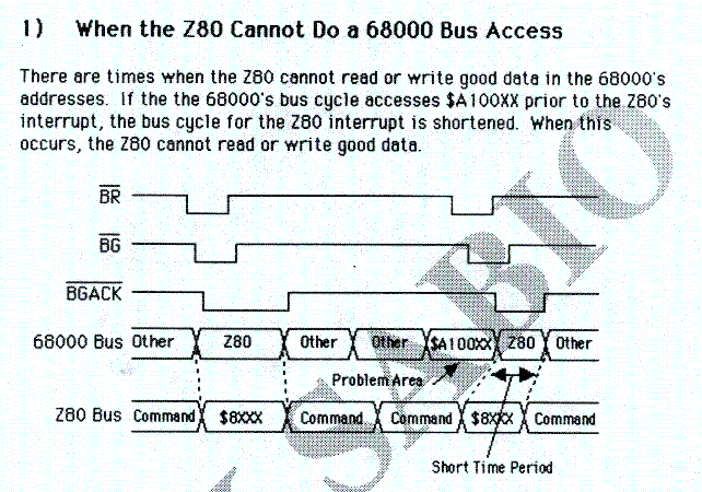
This also could explain why it is strongly suggested to request the z80 bus before accessing IO registers with 68000 (see Addendum 3 at the end of the scanned programmer manual )
As I imagine it, according to the state of these two lines, IO chip read data from one bus and write it to the other bus (or "connect" the two DATA buses to each other)
The Bus Arbitrer is most probably taking care of ALL control signals and address lines (I think that VA1-VA7 and ZA1-ZA7 lines are only used by the IO chip when decoding memory accesses to IO registers mapped at $A10001-$A1001F).
This also could explain why it is strongly suggested to request the z80 bus before accessing IO registers with 68000 (see Addendum 3 at the end of the scanned programmer manual )