Model 1 MD PCB hacks topic
Posted: Wed Oct 29, 2014 3:26 am
I was thinking about this earlier and thought it really deserved its own topic. I've never seen information about this all contained in one place, and I figured people on this board would have a lot of practical background to contribute so why not.
We all know there's a few official board revisions, some pretty rare and some more common. Not including things like the VA7 model 1 board, or the consolidation of custom chips over time, what are some of the more common PCB 'hacks' (jumper wires, additional capacitors/resistors soldered in weird places, etc) that were common on model 1 boards?
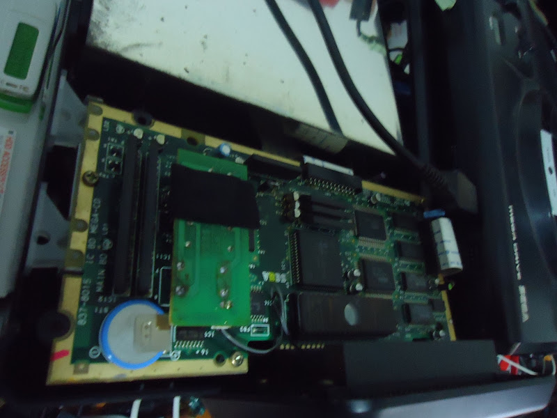
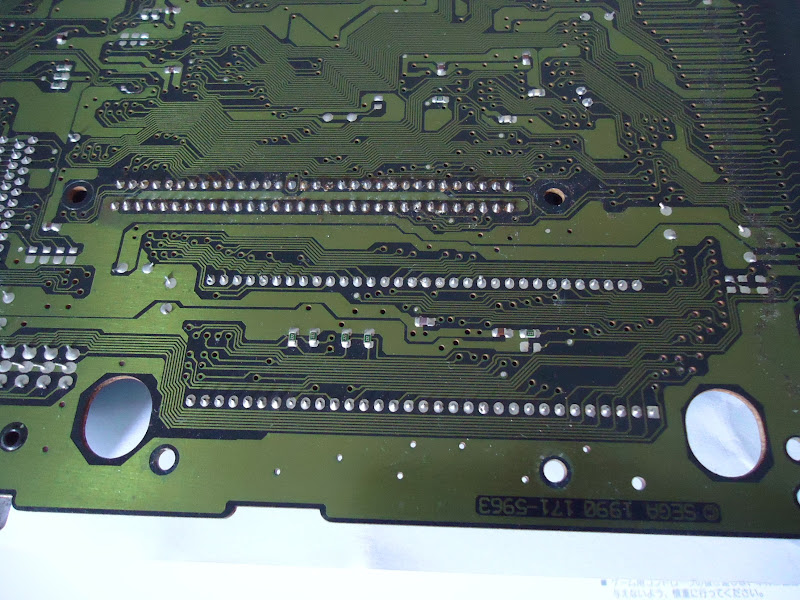
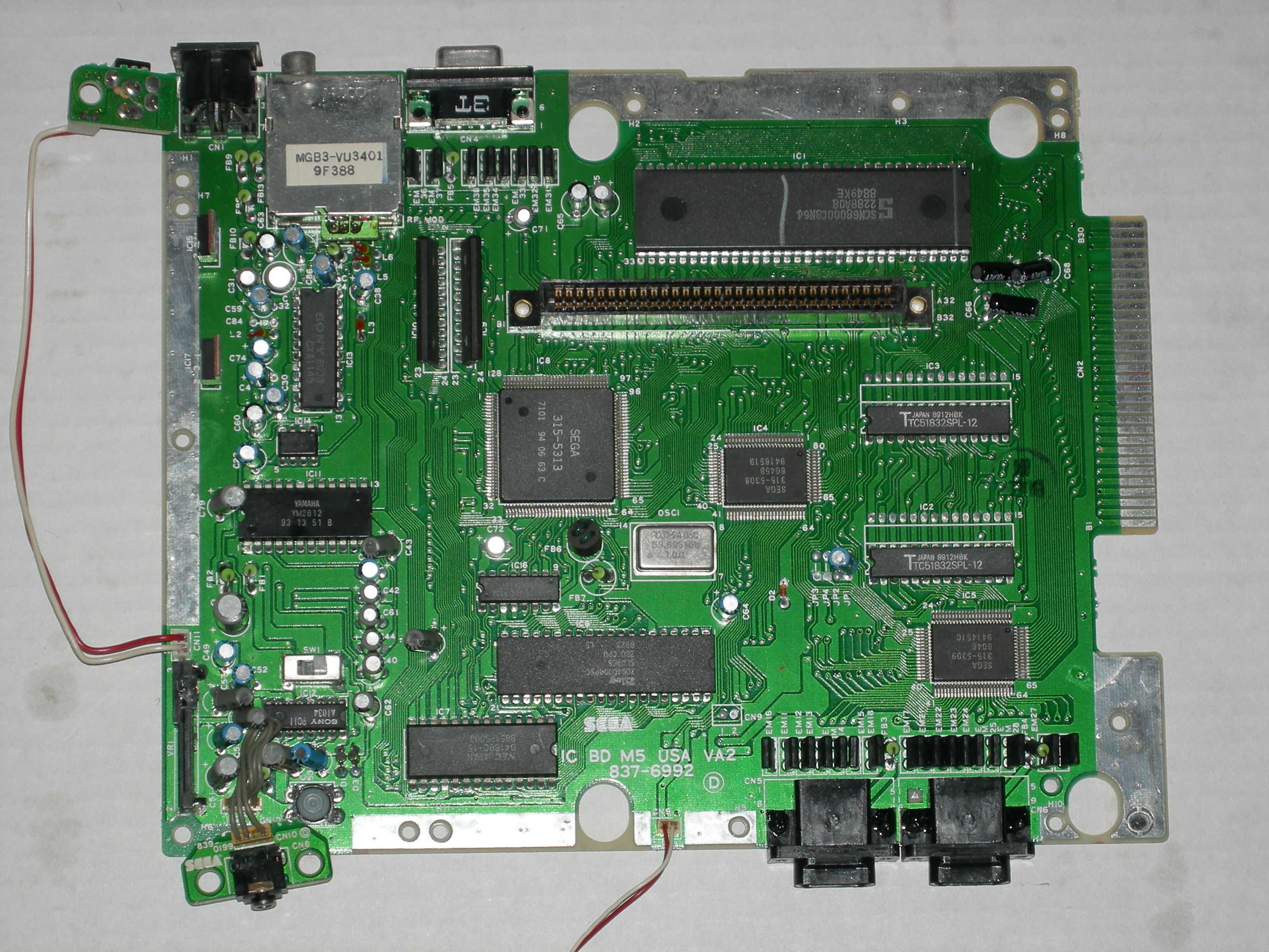
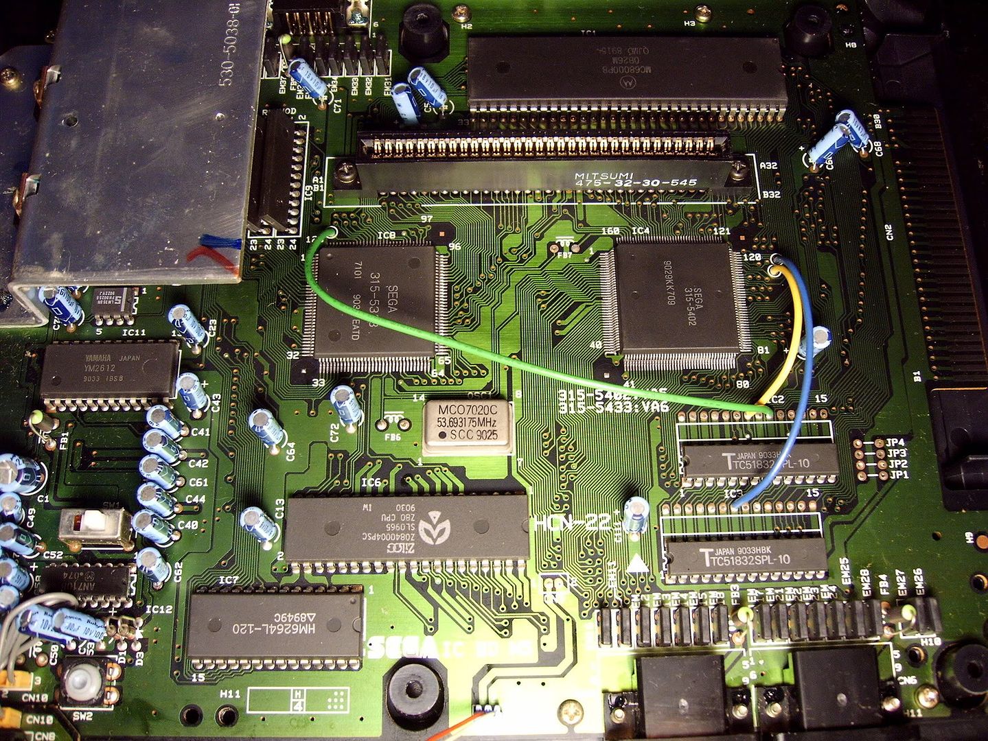
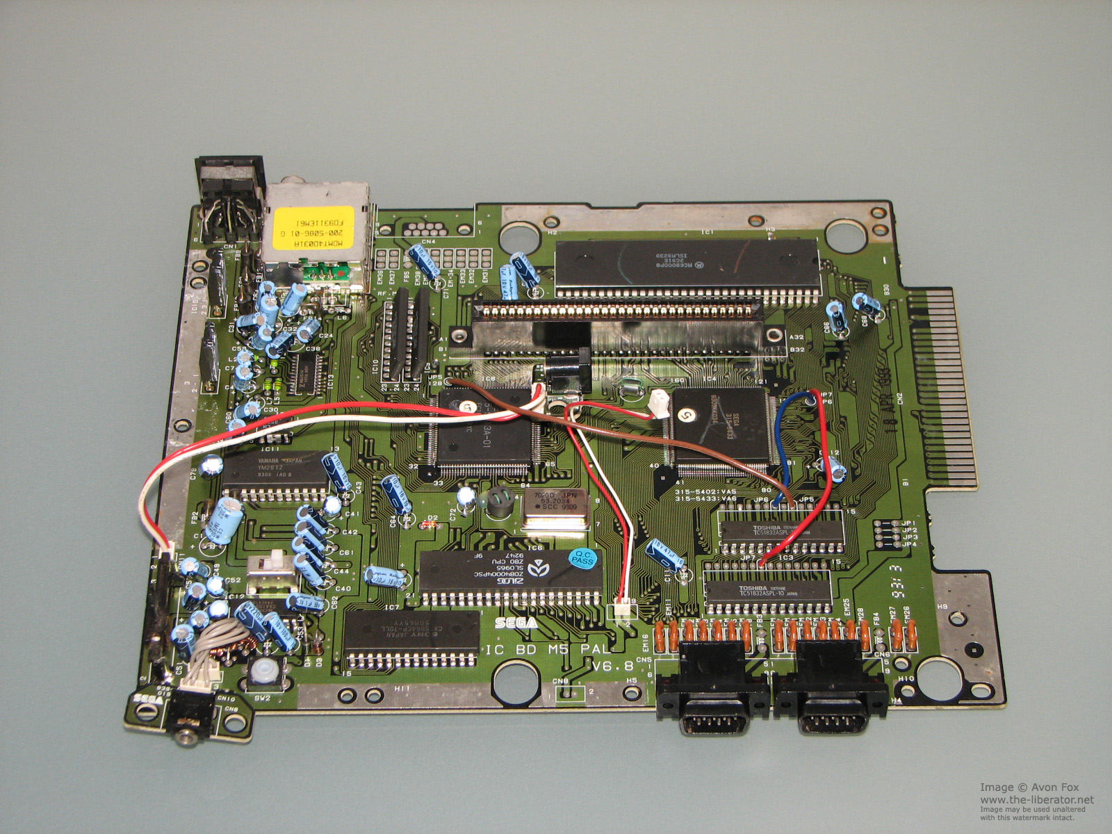
The ones I have seen in person are the VA6 jumper wires, the resistor soldered to the /AS leg of the 68k, a disc capacitor soldered down next to the crystal (didn't notice at first but there were no board through-holes for it and it was attached to a via), and some others including another 68k that had a disc capacitor soldered to one of the legs and to what I guess is a ground plane under the CPU. I have a VA3 board that has a capacitor soldered to the bottom near the VRAM, and one unpopulated capacitor space on top.
I know there others, like the little daughterboard on Japanese launch day boards and probably ones I'm not even aware of.
I'm curious why some of these were obviously patched in at a later stage in production. I understand that PCB design doesn't always come out perfect, especially when you're ramping up design of a popular game console.
The one I'm personally most interested in is the VA3 jumper wires hooked to the RAM & to another pad near the VDP, as they obviously anticipated this one--why else would they print on jumper pads instead of just printing the 'fix' on the board? My guess is it has something to do with available RAM parts and their speed as 2 of the wires go to the RAM's /CE but I'd love to know as I'm not super knowledgeable in such things. Especially since I have a board I added some 'new' (well, NOS) RAM to that isn't working correctly right now.
http://i.imgur.com/GvR7hvH.jpg
The main reason I think this topic is worth having around is that it makes for good service notes as well--later fixes made on later boards might be beneficial to improving older revisions as well. Particularly, as much as I love the model 1 Genesis, it sometimes seems like a really finicky, somewhat shoddy board. It might be component age or EM interference or some other factor, but MD2's seem more 'solid.' (I can't leave a mobile phone anywhere near a model 1 if it is in use, for instance.) Of course, some of this might be having more bugs worked out or more modern fabrication processes.
Hell, if I get bored enough tomorrow I might try 'undoing' the jumper wire fix on one of my other va6 boards just to see what happens.
We all know there's a few official board revisions, some pretty rare and some more common. Not including things like the VA7 model 1 board, or the consolidation of custom chips over time, what are some of the more common PCB 'hacks' (jumper wires, additional capacitors/resistors soldered in weird places, etc) that were common on model 1 boards?
The ones I have seen in person are the VA6 jumper wires, the resistor soldered to the /AS leg of the 68k, a disc capacitor soldered down next to the crystal (didn't notice at first but there were no board through-holes for it and it was attached to a via), and some others including another 68k that had a disc capacitor soldered to one of the legs and to what I guess is a ground plane under the CPU. I have a VA3 board that has a capacitor soldered to the bottom near the VRAM, and one unpopulated capacitor space on top.
I know there others, like the little daughterboard on Japanese launch day boards and probably ones I'm not even aware of.
I'm curious why some of these were obviously patched in at a later stage in production. I understand that PCB design doesn't always come out perfect, especially when you're ramping up design of a popular game console.
The one I'm personally most interested in is the VA3 jumper wires hooked to the RAM & to another pad near the VDP, as they obviously anticipated this one--why else would they print on jumper pads instead of just printing the 'fix' on the board? My guess is it has something to do with available RAM parts and their speed as 2 of the wires go to the RAM's /CE but I'd love to know as I'm not super knowledgeable in such things. Especially since I have a board I added some 'new' (well, NOS) RAM to that isn't working correctly right now.
http://i.imgur.com/GvR7hvH.jpg
The main reason I think this topic is worth having around is that it makes for good service notes as well--later fixes made on later boards might be beneficial to improving older revisions as well. Particularly, as much as I love the model 1 Genesis, it sometimes seems like a really finicky, somewhat shoddy board. It might be component age or EM interference or some other factor, but MD2's seem more 'solid.' (I can't leave a mobile phone anywhere near a model 1 if it is in use, for instance.) Of course, some of this might be having more bugs worked out or more modern fabrication processes.
Hell, if I get bored enough tomorrow I might try 'undoing' the jumper wire fix on one of my other va6 boards just to see what happens.


